- 您现在的位置:买卖IC网 > PDF目录15170 > ISL6558IBZ (Intersil)IC REG CTRLR BUCK PWM 16-SOIC PDF资料下载
参数资料
| 型号: | ISL6558IBZ |
| 厂商: | Intersil |
| 文件页数: | 8/16页 |
| 文件大小: | 0K |
| 描述: | IC REG CTRLR BUCK PWM 16-SOIC |
| 标准包装: | 480 |
| PWM 型: | 控制器 |
| 输出数: | 1 |
| 频率 - 最大: | 1.5MHz |
| 占空比: | 75% |
| 电源电压: | 4.75 V ~ 5.25 V |
| 降压: | 是 |
| 升压: | 无 |
| 回扫: | 无 |
| 反相: | 无 |
| 倍增器: | 无 |
| 除法器: | 无 |
| Cuk: | 无 |
| 隔离: | 无 |
| 工作温度: | -40°C ~ 85°C |
| 封装/外壳: | 16-SOIC(0.154",3.90mm 宽) |
| 包装: | 管件 |
�� �
�
�ISL6558�
�Operation�
�Figure� 1� shows� a� simplified� diagram� of� the� voltage� regulation�
�and� current� control� loops� for� a� two-phase� converter.� Both�
�voltage� and� current� feedback� are� used� to� precisely� regulate�
�output� voltage� and� tightly� control� phase� currents,� I� L1� and� I� L2� ,�
�of� the� two� power� channels.�
�Voltage� Loop�
�Output� voltage� feedback� is� applied� via� the� resistor�
�combination� of� R� FB� and� R� OS� to� the� inverting� input� of� the�
�error� amplifier.� This� signal� drives� the� error� amplifier� output�
�high� or� low,� depending� upon� the� scaled� output� voltage� in�
�relation� to� the� reference� voltage� of� 0.8V.� The� amplifier� output�
�voltage� is� distributed� among� the� active� PWM� channels� and�
�summed� with� their� individual� current� correction� signals.� The�
�resultant� signal,� V� ERROR� ,� is� fed� into� the� PWM� control�
�circuitry� for� each� channel.� Within� this� block,� the� signal� is�
�compared� with� a� sawtooth� ramp� signal.� The� sawtooth� ramp�
�signal� applied� to� each� channel� is� out-of-phase� with� the�
�others.� The� resulting� duty� cycle� signal� for� each� channel� is�
�determined� by� the� movement� of� the� correction� voltage,�
�V� ERROR� ,� relative� to� the� sawtooth� ramp.� The� individual� duty�
�cycle� signals� are� sent� to� their� respective� HIP660x� gate�
�drivers� from� the� PWM� pins.� The� HIP660x� gate� drivers� then�
�switch� their� upper� and� lower� MOSFETs� in� accordance� to� this�
�PWM� signal.�
�Current� Loop�
�The� current� control� loop� keeps� the� channel� currents� in�
�balance.� During� the� PWM� off-time� of� each� channel,� the�
�voltage� developed� across� the� r� DS(ON)� of� the� lower� MOSFET�
�is� sampled.� The� current� is� scaled� by� the� R� ISEN� resistor� and�
�provides� feedback� proportional� to� the� output� current� of� each�
�channel.� The� scaled� output� current� from� all� active� channels�
�are� combined� to� create� an� average� current� reference,�
�I� TOTAL� ,� relative� to� the� converter’s� total� output� current.� This�
�pulse� width� to� lower� the� output� current� contribution� by�
�Channel� 2,� while� doing� the� opposite� to� Channel� 1.�
�Droop� Compensation�
�Microprocessors� and� other� peripherals� tend� to� change� their�
�load� current� demands� often� from� near� no-load� to� full� load�
�during� operation.� These� same� devices� require� minimal�
�output� voltage� deviation� from� nominal� during� a� load� step.�
�A� high� di/dt� load� step� will� cause� an� output� voltage� spike.� The�
�amplitude� of� the� spike� is� dictated� by� the� output� capacitor�
�ESR� (effective� series� resistance)� multiplied� by� the� load� step�
�magnitude� and� output� capacitor� ESL� (equivalent� series�
�inductance)� times� the� load� step� di/dt.� A� positive� load� step�
�produces� a� negative� output� voltage� spike� and� visa� versa.�
�The� overall� output� voltage� deviation� could� exceed� the�
�tolerance� of� some� devices.� One� widely� accepted� solution� to�
�this� problem� is� output� voltage� “droop”� or� active� voltage�
�positioning.�
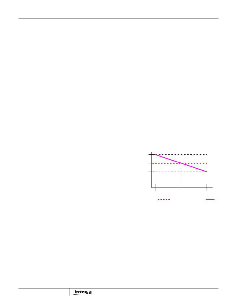
�Droop� is� set� relative� to� the� output� voltage� tolerance�
�specifications� of� the� load� device.� Most� device� tolerance�
�specifications� straddle� the� nominal� output� voltage.� At� no-�
�load,� the� output� voltage� is� set� to� a� slightly� higher� than�
�nominal� level,� V� OUT,NL� .� At� full� load,� the� output� voltage� is� set�
�to� a� slightly� lower� than� nominal� level,� V� OUT,FL� .� The� result� is�
�a� desire� to� have� an� output� voltage� characteristic� as� shown�
�by� the� load� line� in� Figure� 2.�
�V� OUT,NL�
�V� OUT,NOM�
�V� OUT,FL�
�signal� is� then� subtracted� from� the� individual� channel� scaled�
�I� OUT,NL�
�I� OUT,MID�
�I� OUT,MAX�
�output� currents� to� produce� a� current� correction� signal� for�
�each� channel.� The� current� correction� signal� keeps� each�
�NOMINAL� LOAD� LINE�
�DROOP� LOAD� LIN� E�
�channel’s� output� current� contribution� balanced� relative� to� the�
�other� active� channels.� Each� current� correction� signal� is� then�
�subtracted� from� the� error� amplifier� output� and� fed� to� the�
�individual� channel� PWM� circuits.�
�For� example,� assume� the� voltage� sampled� across� Q4� in�
�Figure� 1� is� higher� than� that� sampled� across� Q2.� The� ISEN2�
�current� would� be� higher� then� ISEN1.� When� the� two�
�reference� currents� are� averaged,� they� still� accurately�
�represent� the� total� output� current� of� the� converter.� The�
�reference� current� I� TOTAL� is� then� subtracted� from� the� ISEN�
�currents.� This� results� in� a� positive� offset� for� Channel� 2� and� a�
�negative� offset� for� Channel� 1.� These� offsets� are� subtracted�
�from� the� error� amplifier� signal� and� perform� phase� balance�
�correction.� The� V� ERROR2� signal� is� reduced,� while� V� ERROR1�
�would� be� increased.� The� PWM� circuit� would� then� reduce� the�
�8�
�FIGURE� 2.� SIMPLE� OUTPUT� DEVICE� LOAD� LINE�
�With� droop� implemented� and� a� positive� load� step,� the�
�resulting� negative� output� voltage� spike� begins� from� the� slightly�
�elevated� level� of� V� OUT,NL� .� Similarly,� if� the� load� steps� from� full�
�load,� I� OUT,MAX� ,� back� to� no-load,� I� OUT,NL� ,� the� output� voltage�
�starts� from� the� slightly� lower� V� OUT,FL� position.� These� few�
�millivolts� of� offset� help� reduce� the� size� and� cost� of� output�
�capacitors� required� to� handle� a� given� load� step.�
�Droop� is� an� optional� feature� of� the� ISL6558.� It� is�
�implemented� by� connecting� the� DROOP� and� FB� pins� as�
�shown� in� Figure� 1.� An� internal� current� source,� I� DROOP� ,�
�feeds� out� of� the� DROOP� pin.� The� magnitude� of� I� DROOP� is�
�controlled� by� the� scaled� representation� of� the� total� output�
�current� created� from� the� individual� ISEN� currents.� I� DROOP�
�creates� a� voltage� drop� across� R� FB� and� offsets� the� output�
�FN9027.12�
�June� 21,� 2005�
�相关PDF资料 |
PDF描述 |
|---|---|
| RCM15DTAN-S273 | CONN EDGECARD 30POS R/A .156 SLD |
| ISL6316IRZ-T | IC REG CTRLR BUCK PWM VM 40-QFN |
| VI-J4L-EW-F4 | CONVERTER MOD DC/DC 28V 100W |
| RCM15DTAD-S273 | CONN EDGECARD 30POS R/A .156 SLD |
| CAT1022WI-28-GT3 | IC SUPERVISOR CPU 2K EEPR 8SOIC |
相关代理商/技术参数 |
参数描述 |
|---|---|
| ISL6558IBZ-T | 功能描述:IC REG CTRLR BUCK PWM 16-SOIC RoHS:是 类别:集成电路 (IC) >> PMIC - 稳压器 - DC DC 切换控制器 系列:- 产品培训模块:Lead (SnPb) Finish for COTS Obsolescence Mitigation Program 标准包装:2,500 系列:- PWM 型:电流模式 输出数:1 频率 - 最大:275kHz 占空比:50% 电源电压:18 V ~ 110 V 降压:无 升压:无 回扫:无 反相:无 倍增器:无 除法器:无 Cuk:无 隔离:是 工作温度:-40°C ~ 85°C 封装/外壳:8-SOIC(0.154",3.90mm 宽) 包装:带卷 (TR) |
| ISL6558IR | 功能描述:IC REG CTRLR BUCK PWM 20-QFN RoHS:否 类别:集成电路 (IC) >> PMIC - 稳压器 - DC DC 切换控制器 系列:- 标准包装:4,000 系列:- PWM 型:电压模式 输出数:1 频率 - 最大:1.5MHz 占空比:66.7% 电源电压:4.75 V ~ 5.25 V 降压:是 升压:无 回扫:无 反相:无 倍增器:无 除法器:无 Cuk:无 隔离:无 工作温度:-40°C ~ 85°C 封装/外壳:40-VFQFN 裸露焊盘 包装:带卷 (TR) |
| ISL6558IR-T | 功能描述:IC REG CTRLR BUCK PWM 20-QFN RoHS:否 类别:集成电路 (IC) >> PMIC - 稳压器 - DC DC 切换控制器 系列:- 标准包装:4,000 系列:- PWM 型:电压模式 输出数:1 频率 - 最大:1.5MHz 占空比:66.7% 电源电压:4.75 V ~ 5.25 V 降压:是 升压:无 回扫:无 反相:无 倍增器:无 除法器:无 Cuk:无 隔离:无 工作温度:-40°C ~ 85°C 封装/外壳:40-VFQFN 裸露焊盘 包装:带卷 (TR) |
| ISL6558IRZ | 功能描述:IC REG CTRLR BUCK PWM 20-QFN RoHS:是 类别:集成电路 (IC) >> PMIC - 稳压器 - DC DC 切换控制器 系列:- 产品培训模块:Lead (SnPb) Finish for COTS Obsolescence Mitigation Program 标准包装:2,500 系列:- PWM 型:电流模式 输出数:1 频率 - 最大:275kHz 占空比:50% 电源电压:18 V ~ 110 V 降压:无 升压:无 回扫:无 反相:无 倍增器:无 除法器:无 Cuk:无 隔离:是 工作温度:-40°C ~ 85°C 封装/外壳:8-SOIC(0.154",3.90mm 宽) 包装:带卷 (TR) |
| ISL6558IRZA | 功能描述:IC REG CTRLR BUCK PWM 20-QFN RoHS:是 类别:集成电路 (IC) >> PMIC - 稳压器 - DC DC 切换控制器 系列:- 产品培训模块:Lead (SnPb) Finish for COTS Obsolescence Mitigation Program 标准包装:2,500 系列:- PWM 型:电流模式 输出数:1 频率 - 最大:275kHz 占空比:50% 电源电压:18 V ~ 110 V 降压:无 升压:无 回扫:无 反相:无 倍增器:无 除法器:无 Cuk:无 隔离:是 工作温度:-40°C ~ 85°C 封装/外壳:8-SOIC(0.154",3.90mm 宽) 包装:带卷 (TR) |
发布紧急采购,3分钟左右您将得到回复。