参数资料
| 型号: | ISL6558IR-T |
| 厂商: | Intersil |
| 文件页数: | 12/16页 |
| 文件大小: | 0K |
| 描述: | IC REG CTRLR BUCK PWM 20-QFN |
| 标准包装: | 6,000 |
| PWM 型: | 控制器 |
| 输出数: | 1 |
| 频率 - 最大: | 1.5MHz |
| 占空比: | 75% |
| 电源电压: | 4.75 V ~ 5.25 V |
| 降压: | 是 |
| 升压: | 无 |
| 回扫: | 无 |
| 反相: | 无 |
| 倍增器: | 无 |
| 除法器: | 无 |
| Cuk: | 无 |
| 隔离: | 无 |
| 工作温度: | -40°C ~ 85°C |
| 封装/外壳: | 20-VQFN 裸露焊盘 |
| 包装: | 带卷 (TR) |
�� �
�
�ISL6558�
�from� reacting� to� undervoltage� or� overvoltage� conditions� at�
�the� proper� time.�
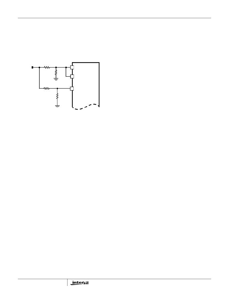
�If� the� output� voltage� is� not� the� same� as� the� internal� 0.8V�
�reference,� then� a� resistor� divider� scaled� like� the� FB� resistors�
�is� required� as� shown� is� Figure� 8.� Otherwise,� the� output�
�voltage� should� be� tied� directly� back� to� the� VSEN� pin� without�
�a� resistor� divider.�
�There� are� two� sets� of� critical� components� in� a� DC-DC�
�converter� using� a� ISL6558� controller� and� HIP660x� gate�
�drivers.� The� switching� components� are� the� most� critical�
�because� they� switch� large� amounts� of� energy,� and� therefore�
�tend� to� generate� equally� large� amounts� of� noise.� Next� are�
�the� small� signal� components� which� connect� to� sensitive�
�nodes� or� supply� critical� bypassing� current� and� signal�
�coupling.�
�V� OUT�
�R� FB�
�R� OS�
�FB�
�DROOP�
�A� multi-layer� printed� circuit� board� is� recommended.� Figure� 9�
�shows� the� connections� of� the� critical� components� for� one�
�output� channel� of� the� converter.� Note� that� capacitors� C� IN�
�and� C� OUT� could� each� represent� numerous� physical�
�capacitors.� Dedicate� one� solid� layer,� usually� the� middle� layer�
�R� FB�
�VSEN�
�of� the� PC� board,� for� a� ground� plane� and� make� all� critical�
�component� ground� connections� with� vias� to� this� layer.�
�R� OS�
�ISL6558�
�Dedicate� another� solid� layer� as� a� power� plane� and� break� this�
�plane� into� smaller� islands� of� common� voltage� levels.� Keep�
�the� metal� runs� from� the� PHASE� terminal� to� the� output�
�inductor� short.� The� power� plane� should� support� the� input�
�FIGURE� 8.� VSEN� RESISTOR� DIVIDER� CONFIGURATION�
�PGOOD� SIGNAL�
�The� undervoltage� comparator� and� overvoltage� latch� feed�
�into� the� power� good� monitor� and� are� NOR’d� together.� If�
�either� indicates� a� fault,� the� power� good� monitor� triggers� the�
�PGOOD� output� low.� A� high� on� this� open� drain� pin� indicates�
�proper� output� voltage.�
�Application� Guidelines�
�Layout� Considerations�
�Layout� is� very� important� in� high� frequency� switching�
�converter� design.� With� MOSFETs� switching� efficiently� at�
�greater� than� 100kHz,� the� resulting� current� transitions� from�
�one� device� to� another� cause� voltage� spikes� across� the�
�interconnecting� impedances� and� parasitic� circuit� elements.�
�These� voltage� spikes� can� degrade� efficiency,� radiate� noise�
�into� the� circuit,� and� lead� to� device� overvoltage� stress.�
�Careful� component� layout� and� printed� circuit� design�
�minimizes� the� voltage� spikes� in� the� converter.�
�As� an� example,� consider� the� turnoff� transition� of� the� PWM�
�upper� MOSFET.� Prior� to� turnoff,� the� upper� MOSFET� was�
�carrying� the� channel� current.� During� turnoff,� current� stops�
�flowing� in� the� upper� MOSFET� and� is� picked� up� by� the� lower�
�MOSFET.� Any� inductance� in� the� switched� current� path�
�generates� a� large� voltage� spike� during� the� switching� interval.�
�Careful� component� selection,� tight� layout� of� the� critical�
�components,� and� short,� wide� circuit� traces� minimize� the�
�magnitude� of� voltage� spikes.�
�12�
�power� and� output� power� nodes.� Use� copper� filled� polygons�
�on� the� top� and� bottom� circuit� layers� for� the� phase� nodes.�
�Use� the� remaining� printed� circuit� layers� for� small� signal�
�wiring.� The� wiring� traces� from� the� HIP660x� driver� to� the�
�power� MOSFET� gates� and� source� should� be� sized� to� carry�
�at� least� 1A� of� current.�
�The� switching� components� and� HIP660x� gate� drivers� should�
�be� placed� first.� Locate� the� input� capacitors� close� to� the�
�power� switches.� Minimize� the� length� of� the� connections�
�between� the� input� capacitors,� C� IN� ,� and� the� power� switches.�
�Position� both� the� ceramic� and� bulk� input� capacitors� as� close�
�to� the� upper� MOSFET� drain� as� possible.� Locate� the� output�
�inductors� and� output� capacitors� between� the� MOSFETs� and�
�the� load.� Place� the� HIP660x� gate� drivers� close� to� their�
�respective� channel� MOSFETs.�
�The� critical� small� signal� components� include� the� bypass�
�capacitors� for� VCC� on� the� ISL6558� controller� as� well� as�
�those� on� VCC� and� PVCC� of� the� HIP660x� gate� drivers.�
�Position� the� bypass� capacitors,� C� BP� ,� close� to� the� device�
�pins.� It� is� especially� important� to� place� the� feedback�
�resistors,� R� FB� and� R� OS� ,� and� compensation� components,� R� C�
�and� C� C� ,� associated� with� the� input� to� the� error� amplifier� close�
�to� the� FB� and� COMP� pins.� Care� should� be� taken� in� routing�
�the� current� sense� lines� such� that� the� ISEN� resistors� are�
�close� to� their� respective� pins� on� the� controller.� Resistor� R� T� ,�
�which� sets� the� oscillator� frequency,� should� be� positioned�
�near� the� FS/EN� pin.�
�FN9027.12�
�June� 21,� 2005�
�相关PDF资料 |
PDF描述 |
|---|---|
| ISL6559CBZ-T | IC REG CTRLR BUCK PWM VM 28-SOIC |
| ISL6561CR-T | IC CTRLR PWM MULTIPHASE 40-QFN |
| ISL6563IR-T | IC CTRLR PWM MULTIPHASE 24-QFN |
| ISL6564AIRZ | IC REG CTRLR BUCK PWM VM 40-QFN |
| ISL6564IR-T | IC REG CTRLR BUCK PWM VM 40-QFN |
相关代理商/技术参数 |
参数描述 |
|---|---|
| ISL6558IRZ | 功能描述:IC REG CTRLR BUCK PWM 20-QFN RoHS:是 类别:集成电路 (IC) >> PMIC - 稳压器 - DC DC 切换控制器 系列:- 产品培训模块:Lead (SnPb) Finish for COTS Obsolescence Mitigation Program 标准包装:2,500 系列:- PWM 型:电流模式 输出数:1 频率 - 最大:275kHz 占空比:50% 电源电压:18 V ~ 110 V 降压:无 升压:无 回扫:无 反相:无 倍增器:无 除法器:无 Cuk:无 隔离:是 工作温度:-40°C ~ 85°C 封装/外壳:8-SOIC(0.154",3.90mm 宽) 包装:带卷 (TR) |
| ISL6558IRZA | 功能描述:IC REG CTRLR BUCK PWM 20-QFN RoHS:是 类别:集成电路 (IC) >> PMIC - 稳压器 - DC DC 切换控制器 系列:- 产品培训模块:Lead (SnPb) Finish for COTS Obsolescence Mitigation Program 标准包装:2,500 系列:- PWM 型:电流模式 输出数:1 频率 - 最大:275kHz 占空比:50% 电源电压:18 V ~ 110 V 降压:无 升压:无 回扫:无 反相:无 倍增器:无 除法器:无 Cuk:无 隔离:是 工作温度:-40°C ~ 85°C 封装/外壳:8-SOIC(0.154",3.90mm 宽) 包装:带卷 (TR) |
| ISL6558IRZA-T | 功能描述:IC REG CTRLR BUCK PWM 20-QFN RoHS:是 类别:集成电路 (IC) >> PMIC - 稳压器 - DC DC 切换控制器 系列:- 产品培训模块:Lead (SnPb) Finish for COTS Obsolescence Mitigation Program 标准包装:2,500 系列:- PWM 型:电流模式 输出数:1 频率 - 最大:275kHz 占空比:50% 电源电压:18 V ~ 110 V 降压:无 升压:无 回扫:无 反相:无 倍增器:无 除法器:无 Cuk:无 隔离:是 工作温度:-40°C ~ 85°C 封装/外壳:8-SOIC(0.154",3.90mm 宽) 包装:带卷 (TR) |
| ISL6558IRZA-TK | 功能描述:IC REG CTRLR BUCK PWM 20-QFN RoHS:是 类别:集成电路 (IC) >> PMIC - 稳压器 - DC DC 切换控制器 系列:- 产品培训模块:Lead (SnPb) Finish for COTS Obsolescence Mitigation Program 标准包装:2,500 系列:- PWM 型:电流模式 输出数:1 频率 - 最大:275kHz 占空比:50% 电源电压:18 V ~ 110 V 降压:无 升压:无 回扫:无 反相:无 倍增器:无 除法器:无 Cuk:无 隔离:是 工作温度:-40°C ~ 85°C 封装/外壳:8-SOIC(0.154",3.90mm 宽) 包装:带卷 (TR) |
| ISL6558IRZR5240 | 功能描述:IC REG CTRLR BUCK PWM 20-QFN RoHS:是 类别:集成电路 (IC) >> PMIC - 稳压器 - DC DC 切换控制器 系列:- 产品培训模块:Lead (SnPb) Finish for COTS Obsolescence Mitigation Program 标准包装:2,500 系列:- PWM 型:电流模式 输出数:1 频率 - 最大:275kHz 占空比:50% 电源电压:18 V ~ 110 V 降压:无 升压:无 回扫:无 反相:无 倍增器:无 除法器:无 Cuk:无 隔离:是 工作温度:-40°C ~ 85°C 封装/外壳:8-SOIC(0.154",3.90mm 宽) 包装:带卷 (TR) |
发布紧急采购,3分钟左右您将得到回复。