- 您现在的位置:买卖IC网 > PDF目录15063 > ISL6558IR (Intersil)IC REG CTRLR BUCK PWM 20-QFN PDF资料下载
参数资料
| 型号: | ISL6558IR |
| 厂商: | Intersil |
| 文件页数: | 14/16页 |
| 文件大小: | 0K |
| 描述: | IC REG CTRLR BUCK PWM 20-QFN |
| 标准包装: | 60 |
| PWM 型: | 控制器 |
| 输出数: | 1 |
| 频率 - 最大: | 1.5MHz |
| 占空比: | 75% |
| 电源电压: | 4.75 V ~ 5.25 V |
| 降压: | 是 |
| 升压: | 无 |
| 回扫: | 无 |
| 反相: | 无 |
| 倍增器: | 无 |
| 除法器: | 无 |
| Cuk: | 无 |
| 隔离: | 无 |
| 工作温度: | -40°C ~ 85°C |
| 封装/外壳: | 20-VQFN 裸露焊盘 |
| 包装: | 管件 |
�� �
�
�ISL6558�
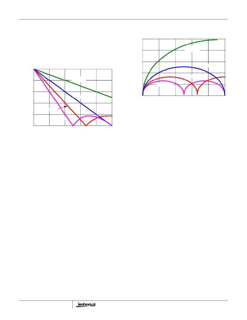
�The� total� output� ripple� current� can� be� determined� from� the�
�curves� in� Figure� 10.� They� provide� the� total� ripple� current� as� a�
�function� of� duty� cycle� and� number� of� active� channels,�
�normalized� to� the� parameter� K� NORM� at� zero� duty� cycle.�
�value� found� and� the� result� is� the� RMS� input� current� whi� c� h�
�must� be� supported� by� the� input� capacitors.�
�0.5�
�K� NORM� =� ---------------------�
�V� OUT�
�LxF� SW�
�where� L� is� the� channel� inductor� value.�
�(EQ.� 11)�
�0.4�
�0.3�
�SINGLE�
�CHANNEL�
�2 CHANNEL�
�1.0�
�0.2�
�0.8�
�0.6�
�SINGLE�
�CHANNEL�
�0.1�
�4 CHANNEL�
�3� CHANNEL�
�2 CHANNEL�
�0�
�0�
�0.1�
�0.2�
�0.3�
�0.4�
�0.5�
�0.4�
�0.2�
�0�
�3 CHANNEL�
�4 CHANNEL�
�DUTY� CYCLE� (V� O� /V� IN� )�
�FIGURE� 11.� CURRENT� MULTIPLIER� vs� DUTY� CYCLE�
�MOSFET� SELECTION� AND� CONSIDERATIONS�
�The� ISL6558� requires� two� N-Channel� power� MOSFETs� per�
�0�
�0.1�
�0.2� 0.3�
�DUTY� CYCLE� (V� O� /V� IN� )�
�0.4�
�0.5�
�active� channel� or� more� if� parallel� MOSFETs� are� employed.�
�These� MOSFETs� should� be� selected� based� upon� r� DS(ON)� ,�
�FIGURE� 10.� RIPPLE� CURRENT� vs� DUTY� CYCLE�
�Find� the� intersection� of� the� active� channel� curve� and� duty�
�cycle� for� your� particular� application.� The� resulting� ripple�
�current� multiplier� from� the� y-axis� is� then� multiplied� by� the�
�normalization� factor,� K� NORM� ,� to� determine� the� total� output�
�ripple� current� for� the� given� application.�
�total� gate� charge,� and� thermal� management� requirements.�
�In� high-current� PWM� applications,� the� MOSFET� power�
�dissipation,� package� selection� and� heatsink� are� the�
�dominant� design� factors.� The� power� dissipation� includes� two�
�loss� components;� conduction� loss� and� switching� loss.� These�
�losses� are� distributed� between� the� upper� and� lower�
�MOSFETs� according� to� duty� cycle� of� the� converter� (see� the�
�D� I� TOTAL� =� K� NORM� xK� CM�
�(EQ.� 12)�
�equations� below).� The� conduction� losses� are� the� main�
�component� of� power� dissipation� for� the� lower� MOSFETs,� Q2�
�I� O� � r� DS� (� ON� )� � V� OUT�
�I� O� � V� IN� � t� SW� � F� SW�
�P� UPPER� =� ------------------------------------------------------------� +� ----------------------------------------------------------�
�V� IN�
�INPUT� CAPACITOR� SELECTION�
�Use� a� mix� of� input� bypass� capacitors� to� control� the� voltage�
�overshoot� across� the� MOSFETs.� Use� ceramic� capacitors� for�
�the� high� frequency� decoupling� and� bulk� capacitors� to� supply�
�the� RMS� current.� Small� ceramic� capacitors� can� be� placed�
�very� close� to� the� upper� MOSFET� to� suppress� the� voltage�
�induced� in� the� parasitic� circuit� impedances.�
�Two� important� parameters� to� consider� when� selecting� the�
�bulk� input� capacitor� are� the� voltage� rating� and� the� RMS�
�current� rating.� For� reliable� operation,� select� a� bulk� capacitor�
�with� voltage� and� current� ratings� above� the� maximum� input�
�voltage� and� largest� RMS� current� required� by� the� circuit.� The�
�capacitor� voltage� rating� should� be� at� least� 1.25� times� greater�
�than� the� maximum� input� voltage� and� a� voltage� rating� of� 1.5�
�times� is� a� conservative� guideline.� The� RMS� current�
�requirement� for� a� converter� design� can� be� approximated� with�
�the� aid� of� Figure� 11.� Follow� the� curve� for� the� number� of� active�
�channels� in� the� converter� design.� Next� determine� the� duty�
�and� Q4� of� Figure� 1.� Only� the� upper� MOSFETs,� Q1� and� Q3�
�have� significant� switching� losses,� since� the� lower� device� turn�
�on� and� off� into� near� zero� voltage.�
�The� following� equations� assume� linear� voltage-current�
�transitions� and� do� not� model� power� loss� due� to� the� reverse-�
�recovery� of� the� lower� MOSFETs� body� diode.� The� gate-�
�charge� losses� are� dissipated� in� the� HIP660x� drivers� and�
�don’t� heat� the� MOSFETs.� However,� large� gate-charge�
�increases� the� switching� time,� t� SW� which� increases� the� upper�
�MOSFET� switching� losses.� Ensure� that� both� MOSFETs� are�
�within� their� maximum� junction� temperature� at� high� ambient�
�temperature� by� calculating� the� temperature� rise� according� to�
�package� thermal-resistance� specifications.� A� separate�
�heatsink� may� be� necessary� depending� upon� MOSFET�
�power,� package� type,� ambient� temperature� and� air� flow.�
�2�
�2�
�(EQ.� 13)�
�I� O� ×� r� DS� (� ON� )� ×� (� V� IN� –� V� OUT� )�
�P� LOWER� =� ---------------------------------------------------------------------------------�
�cycle� for� the� converter� and� find� the� intersection� of� this� value�
�and� the� active� channel� curve.� Find� the� corresponding� y-axis�
�value,� which� is� the� current� multiplier.� Multiply� the� total� full� load�
�output� current,� not� the� channel� value,� by� the� current� multiplier�
�14�
�2�
�V� IN�
�(EQ.� 14)�
�FN9027.12�
�June� 21,� 2005�
�相关PDF资料 |
PDF描述 |
|---|---|
| X4043PIZ-2.7A | IC SUPERVISOR CPU 4K EE 8-DIP |
| ISL6558IB-T | IC REG CTRLR BUCK PWM 16-SOIC |
| ISL6558IB | IC REG CTRLR BUCK PWM 16-SOIC |
| X4043PIZ-2.7 | IC SUPERVISOR CPU 4K EE 8-DIP |
| ISL6558CR-T | IC REG CTRLR BUCK PWM 20-QFN |
相关代理商/技术参数 |
参数描述 |
|---|---|
| ISL6558IR-T | 功能描述:IC REG CTRLR BUCK PWM 20-QFN RoHS:否 类别:集成电路 (IC) >> PMIC - 稳压器 - DC DC 切换控制器 系列:- 标准包装:4,000 系列:- PWM 型:电压模式 输出数:1 频率 - 最大:1.5MHz 占空比:66.7% 电源电压:4.75 V ~ 5.25 V 降压:是 升压:无 回扫:无 反相:无 倍增器:无 除法器:无 Cuk:无 隔离:无 工作温度:-40°C ~ 85°C 封装/外壳:40-VFQFN 裸露焊盘 包装:带卷 (TR) |
| ISL6558IRZ | 功能描述:IC REG CTRLR BUCK PWM 20-QFN RoHS:是 类别:集成电路 (IC) >> PMIC - 稳压器 - DC DC 切换控制器 系列:- 产品培训模块:Lead (SnPb) Finish for COTS Obsolescence Mitigation Program 标准包装:2,500 系列:- PWM 型:电流模式 输出数:1 频率 - 最大:275kHz 占空比:50% 电源电压:18 V ~ 110 V 降压:无 升压:无 回扫:无 反相:无 倍增器:无 除法器:无 Cuk:无 隔离:是 工作温度:-40°C ~ 85°C 封装/外壳:8-SOIC(0.154",3.90mm 宽) 包装:带卷 (TR) |
| ISL6558IRZA | 功能描述:IC REG CTRLR BUCK PWM 20-QFN RoHS:是 类别:集成电路 (IC) >> PMIC - 稳压器 - DC DC 切换控制器 系列:- 产品培训模块:Lead (SnPb) Finish for COTS Obsolescence Mitigation Program 标准包装:2,500 系列:- PWM 型:电流模式 输出数:1 频率 - 最大:275kHz 占空比:50% 电源电压:18 V ~ 110 V 降压:无 升压:无 回扫:无 反相:无 倍增器:无 除法器:无 Cuk:无 隔离:是 工作温度:-40°C ~ 85°C 封装/外壳:8-SOIC(0.154",3.90mm 宽) 包装:带卷 (TR) |
| ISL6558IRZA-T | 功能描述:IC REG CTRLR BUCK PWM 20-QFN RoHS:是 类别:集成电路 (IC) >> PMIC - 稳压器 - DC DC 切换控制器 系列:- 产品培训模块:Lead (SnPb) Finish for COTS Obsolescence Mitigation Program 标准包装:2,500 系列:- PWM 型:电流模式 输出数:1 频率 - 最大:275kHz 占空比:50% 电源电压:18 V ~ 110 V 降压:无 升压:无 回扫:无 反相:无 倍增器:无 除法器:无 Cuk:无 隔离:是 工作温度:-40°C ~ 85°C 封装/外壳:8-SOIC(0.154",3.90mm 宽) 包装:带卷 (TR) |
| ISL6558IRZA-TK | 功能描述:IC REG CTRLR BUCK PWM 20-QFN RoHS:是 类别:集成电路 (IC) >> PMIC - 稳压器 - DC DC 切换控制器 系列:- 产品培训模块:Lead (SnPb) Finish for COTS Obsolescence Mitigation Program 标准包装:2,500 系列:- PWM 型:电流模式 输出数:1 频率 - 最大:275kHz 占空比:50% 电源电压:18 V ~ 110 V 降压:无 升压:无 回扫:无 反相:无 倍增器:无 除法器:无 Cuk:无 隔离:是 工作温度:-40°C ~ 85°C 封装/外壳:8-SOIC(0.154",3.90mm 宽) 包装:带卷 (TR) |
发布紧急采购,3分钟左右您将得到回复。