- 您现在的位置:买卖IC网 > PDF目录15174 > ISL6567IRZ (Intersil)IC REG CTRLR BUCK PWM VM 24-QFN PDF资料下载
参数资料
| 型号: | ISL6567IRZ |
| 厂商: | Intersil |
| 文件页数: | 8/25页 |
| 文件大小: | 0K |
| 描述: | IC REG CTRLR BUCK PWM VM 24-QFN |
| 标准包装: | 75 |
| PWM 型: | 电压模式 |
| 输出数: | 1 |
| 频率 - 最大: | 1.5MHz |
| 占空比: | 66% |
| 电源电压: | 4.9 V ~ 5.5 V |
| 降压: | 是 |
| 升压: | 无 |
| 回扫: | 无 |
| 反相: | 无 |
| 倍增器: | 无 |
| 除法器: | 无 |
| Cuk: | 无 |
| 隔离: | 无 |
| 工作温度: | -40°C ~ 85°C |
| 封装/外壳: | 24-VFQFN 裸露焊盘 |
| 包装: | 管件 |
�� �
�
�ISL6567�
�resistor� network,� allows� the� user� to� adjust� the� threshold�
�hysteresis.� Pulled� below� the� falling� threshold,� this� pin� disables�
�controller� operation,� by� ramping� down� the� SS� voltage� and�
�discharging� the� output.�
�RGND,� VSEN,� and� VDIFF� (Pins� 1,� 2,� and� 4)�
�The� inputs� and� output� of� the� on-board� unity-gain� operational�
�amplifier� intended� for� differential� output� sensing.� Connect�
�RGND� and� VSEN� to� the� output� load’s� local� GND� and� VOUT,�
�respectively;� VDIFF� will� reflect� the� load� voltage� referenced� to�
�the� chip’s� local� ground.� Connect� the� feedback� network� to� the�
�voltage� thus� reflected� at� the� VDIFF� pin.� Should� the� circuit� not�
�allow� implementation� of� remote� sensing,� connect� the� VSEN�
�and� RGND� pins� to� the� physical� place� where� voltage� is� to� be�
�regulated.�
�Connect� the� resistor� divider� setting� the� output� voltage� at� the�
�input� of� the� differential� amplifier.� To� minimize� the� error�
�introduced� by� the� resistance� of� differential� amplifier’s� inputs,�
�select� resistor� divider� values� smaller� than� 1k� Ω� .� VDIFF� is�
�monitored� for� overvoltage� events� and� for� PGOOD� reporting�
�purposes.�
�FB� and� COMP� (Pins� 5� and� 6)�
�The� internal� error� amplifier’s� inverting� input� and� output�
�respectively.� These� pins� are� connected� to� the� external� network�
�used� to� compensate� the� regulator’s� feedback� loop.�
�ISEN1,� ISEN2� (Pins� 17,� 13)�
�These� pins� are� used� to� close� the� current� feedback� loop� and� set�
�the� overcurrent� protection� threshold.� A� resistor� connected�
�between� each� of� these� pins� and� their� corresponding� PHASE�
�pins� determine� a� certain� current� flow� magnitude� during� the�
�lower� MOSFET’s� conduction� interval.� The� resulting� currents�
�established� through� these� resistors� are� used� for� channel�
�current� balancing� and� overcurrent� protection.�
�the� PVCC� pins� provide� the� necessary� bootstrap� charge.�
�Minimize� the� impedance� of� these� connections.�
�PHASE1,� PHASE2� (Pins� 18,� 12)�
�Connect� these� pins� to� the� sources� of� the� upper� MOSFETs.�
�These� pins� are� the� return� path� for� the� upper� MOSFETs’� drives.�
�Minimize� the� impedance� of� these� connections.�
�LGATE1,� LGATE2� (Pins� 16,� 14)�
�These� pins� are� used� to� control� the� lower� MOSFETs� and� are�
�monitored� for� shoot-through� prevention� purposes.� Connect�
�these� pins� to� the� lower� MOSFETs’� gates.� Minimize� the�
�impedance� of� these� connections.�
�SS� (Pin� 23)�
�This� pin� allows� adjustment� of� the� output� voltage� soft-start� ramp�
�rate,� as� well� as� the� hiccup� interval� following� an� overcurrent�
�event.� The� potential� at� this� pin� is� used� as� a� clamp� voltage� for� the�
�internal� error� amplifier’s� non-inverting� input,� regulating� its� rate�
�of� rise� during� start-up.� Connect� this� pin� to� a� capacitor� referenced�
�to� ground.� Small� internal� current� sources� linearly� charge� and�
�discharge� this� capacitor,� leading� to� similar� variation� in� the� ramp�
�up/down� of� the� output� voltage.� While� below� 0.3V,� all� output�
�drives� are� turned� off.� As� this� pin� ramps� up,� the� drives� are� not�
�enabled� but� only� after� the� first� UGATE� pulse� emerges� (avoid�
�draining� the� output,� if� pre-charged).� If� no� UGATE� pulse� are�
�generated� until� the� SS� exceeds� the� top� of� the� oscillator� ramp,� at�
�that� time� all� gate� operation� is� enabled,� allowing� immediate�
�draining� of� the� output,� as� necessary.�
�SS� voltage� has� a� ~0.7V� offset� above� the� reference� clamp,�
�meaning� the� reference� clamp� rises� from� 0V� with� unity� gain�
�correspondence� as� the� SS� pin� exceeds� 0.7V.� For� more�
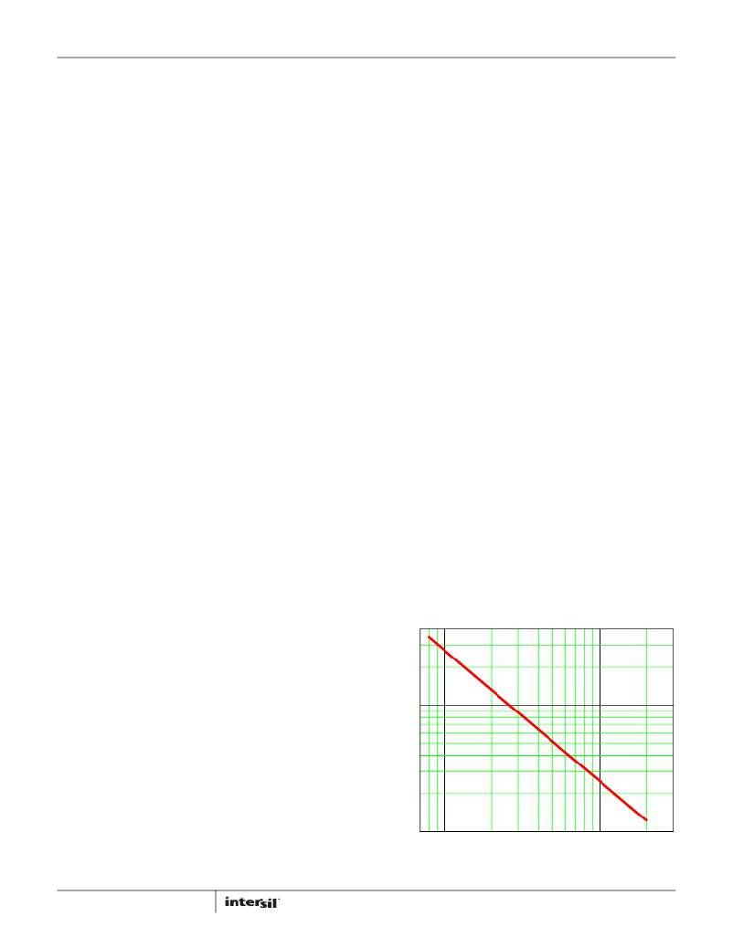
��FS� (Pin� 22)�
�Use� Equation� 1� to� select� the� proper� R� ISEN� resistor:�
�50� μ� A�
�r� DS� (� ON� )� � I� OUT�
�R� ISEN� =� --------------------------------------�
�where:�
�r� DS(ON)� =� lower� MOSFET� drain-source� ON-resistance� (� Ω� )�
�I� OUT� =� channel� maximum� output� current� (A)�
�Read� “Current� Loop”� page� 9,� “Channel-Current� Balance”�
�(EQ.� 1)�
�This� pin� is� used� to� set� the� switching� frequency.� Connect� a�
�resistor,� R� FS� ,� from� this� pin� to� ground� and� size� it� according� to� the�
�graph� in� Figure� 1� or� Equation� 2:�
�(� 10.61� –� (� 1.035� ?� log� (� F� SW� )� )� )� (EQ.� 2)�
�R� FS� =� 10�
�200k�
��information.�
�UGATE1,� UGATE2� (Pins� 19,� 11)�
�Connect� these� pins� to� the� upper� MOSFETs’� gates.� These� pins�
�are� used� to� control� the� upper� MOSFETs� and� are� monitored� for�
�shoot-through� prevention� purposes.� Minimize� the� impedance�
�of� these� connections.� Maximum� individual� channel� duty� cycle�
�is� limited� to� 66%.�
�100k�
�50k�
�20k�
�BOOT1,� BOOT2� (Pins� 20,� 10)�
�These� pins� provide� the� bias� voltage� for� the� upper� MOSFETs’�
�10k�
�100k�
�200k�
�500k�
�1M�
�2M�
�drives.� Connect� these� pins� to� appropriately-chosen� external�
�bootstrap� capacitors.� Internal� bootstrap� diodes� connected� to�
�8�
�SWITCHING� FREQUENCY� (Hz)�
�FIGURE� 1.� SWITCHING� FREQUENCY� vs� R� FS� VALUE�
�FN9243.4�
�August� 9,� 2011�
�相关PDF资料 |
PDF描述 |
|---|---|
| RSA14DTAH | CONN EDGECARD 28POS R/A .125 SLD |
| ISL6567IRZS2698 | IC REG CTRLR BUCK PWM VM 24-QFN |
| VE-25Z-EX-F2 | CONVERTER MOD DC/DC 2V 30W |
| SN331M025ST | CAP ALUM 330UF 25V 20% RADIAL |
| SXR151M100ST | CAP ALUM 150UF 100V 20% RADIAL |
相关代理商/技术参数 |
参数描述 |
|---|---|
| ISL6567IRZS2698 | 功能描述:IC REG CTRLR BUCK PWM VM 24-QFN RoHS:是 类别:集成电路 (IC) >> PMIC - 稳压器 - DC DC 切换控制器 系列:- 产品培训模块:Lead (SnPb) Finish for COTS Obsolescence Mitigation Program 标准包装:2,500 系列:- PWM 型:电流模式 输出数:1 频率 - 最大:275kHz 占空比:50% 电源电压:18 V ~ 110 V 降压:无 升压:无 回扫:无 反相:无 倍增器:无 除法器:无 Cuk:无 隔离:是 工作温度:-40°C ~ 85°C 封装/外壳:8-SOIC(0.154",3.90mm 宽) 包装:带卷 (TR) |
| ISL6567IRZ-T | 功能描述:IC REG CTRLR BUCK PWM VM 24-QFN RoHS:是 类别:集成电路 (IC) >> PMIC - 稳压器 - DC DC 切换控制器 系列:- 产品培训模块:Lead (SnPb) Finish for COTS Obsolescence Mitigation Program 标准包装:2,500 系列:- PWM 型:电流模式 输出数:1 频率 - 最大:275kHz 占空比:50% 电源电压:18 V ~ 110 V 降压:无 升压:无 回扫:无 反相:无 倍增器:无 除法器:无 Cuk:无 隔离:是 工作温度:-40°C ~ 85°C 封装/外壳:8-SOIC(0.154",3.90mm 宽) 包装:带卷 (TR) |
| ISL6567IRZ-TS2698 | 功能描述:IC REG CTRLR BUCK PWM VM 24-QFN RoHS:是 类别:集成电路 (IC) >> PMIC - 稳压器 - DC DC 切换控制器 系列:- 产品培训模块:Lead (SnPb) Finish for COTS Obsolescence Mitigation Program 标准包装:2,500 系列:- PWM 型:电流模式 输出数:1 频率 - 最大:275kHz 占空比:50% 电源电压:18 V ~ 110 V 降压:无 升压:无 回扫:无 反相:无 倍增器:无 除法器:无 Cuk:无 隔离:是 工作温度:-40°C ~ 85°C 封装/外壳:8-SOIC(0.154",3.90mm 宽) 包装:带卷 (TR) |
| ISL6568CR | 功能描述:IC CTRLR PWM BUCK 2PHASE 32-QFN RoHS:否 类别:集成电路 (IC) >> PMIC - 稳压器 - 专用型 系列:- 产品培训模块:Lead (SnPb) Finish for COTS Obsolescence Mitigation Program 标准包装:2,000 系列:- 应用:电源,ICERA E400,E450 输入电压:4.1 V ~ 5.5 V 输出数:10 输出电压:可编程 工作温度:-40°C ~ 85°C 安装类型:表面贴装 封装/外壳:42-WFBGA,WLCSP 供应商设备封装:42-WLP 包装:带卷 (TR) |
| ISL6568CR-T | 功能描述:IC CTRLR PWM BUCK 2PHASE 32-QFN RoHS:否 类别:集成电路 (IC) >> PMIC - 稳压器 - 专用型 系列:- 产品培训模块:Lead (SnPb) Finish for COTS Obsolescence Mitigation Program 标准包装:2,000 系列:- 应用:电源,ICERA E400,E450 输入电压:4.1 V ~ 5.5 V 输出数:10 输出电压:可编程 工作温度:-40°C ~ 85°C 安装类型:表面贴装 封装/外壳:42-WFBGA,WLCSP 供应商设备封装:42-WLP 包装:带卷 (TR) |
发布紧急采购,3分钟左右您将得到回复。