- 您现在的位置:买卖IC网 > PDF目录15061 > ISL6569ACB-T (Intersil)IC REG CTRLR BUCK PWM 24-SOIC PDF资料下载
参数资料
| 型号: | ISL6569ACB-T |
| 厂商: | Intersil |
| 文件页数: | 7/22页 |
| 文件大小: | 0K |
| 描述: | IC REG CTRLR BUCK PWM 24-SOIC |
| 标准包装: | 1,000 |
| PWM 型: | 电流/电压模式 |
| 输出数: | 1 |
| 频率 - 最大: | 2MHz |
| 占空比: | 75% |
| 电源电压: | 4.75 V ~ 5.25 V |
| 降压: | 是 |
| 升压: | 无 |
| 回扫: | 无 |
| 反相: | 无 |
| 倍增器: | 无 |
| 除法器: | 无 |
| Cuk: | 无 |
| 隔离: | 无 |
| 工作温度: | 0°C ~ 70°C |
| 封装/外壳: | 24-SOIC(0.295",7.50mm 宽) |
| 包装: | 带卷 (TR) |
�� �
�
�ISL6569A�
�Functional� Pin� Description�
�VCC�
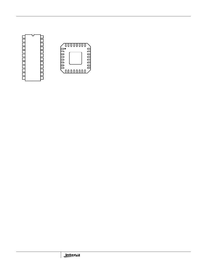
�ISL6569ACB�
�24� LD� SOIC�
�ISL6569ACR�
�32� LEAD� QFN� 5x5�
�Supplies� all� the� power� necessary� to� operate� the� chip.� The� IC�
�starts� to� operate� when� the� voltage� on� this� pin� exceeds� the�
�GND� 1�
�OVP� 2�
�VID4� 3�
�VID3� 4�
�24� EN�
�23� FS/DIS�
�22� PGOOD�
�21� ISEN1�
�VID2�
�NC�
�rising� POR� threshold� and� shuts� down� when� the� voltage� on�
�this� pin� drops� below� the� falling� POR� threshold.� Connect� this�
�pin� directly� to� a� +5V� supply� or� through� a� series� 255� ?� resistor�
�to� a� +12V� supply.�
�VID2� 5�
�VID1� 6�
�VID0� 7�
�OFS� 8�
�COMP� 9�
�FB� 10�
�20� PWM1�
�19� PWM2�
�18� GND�
�17� ISEN2�
�16� VCC�
�15� GND�
�VID1�
�VID0�
�NC�
�OFS�
�COMP�
�FB�
�NC�
�GND�
�BOTTOM�
�SIDE� PAD�
�NC�
�ISEN1�
�PWM1�
�PWM2�
�GND�
�ISEN2�
�NC�
�ISEN1,� ISEN2�
�Current� sense� inputs.� A� resistor� connected� between� these�
�pins� and� their� respective� phase� nodes� sets� a� current�
�proportional� to� the� current� in� the� lower� MOSFET� during� it’s�
�conduction� interval.� This� current� is� used� as� a� reference� for�
�IOUT� 11�
�VDIFF� 12�
�14� RGND�
�13� VSEN�
�channel� balancing,� load� sharing,� protection,� and� load-line�
�droop.�
�GND�
�Bias� and� reference� ground� for� the� IC.�
�OVP�
�Over-voltage� protection� pin.� This� pin� is� pulled� to� VCC� and� is�
�latched� when� an� over-voltage� condition� is� detected.� Connect�
�this� pin� to� the� gate� of� an� SCR� or� MOSFET� tied� across� V� IN�
�and� ground.� A� fuse� must� be� placed� upstream� to� open� the�
�input� supply� rail� and� prevent� damage� to� the� load� device.�
�VID4,� VID3,� VID2,� VID1,� VID0�
�The� state� of� these� five� inputs� program� the� internal� DAC,�
�which� provides� the� reference� voltage� for� output� regulation.�
�Connect� these� pins� to� either� open-drain� or� active� pull-up�
�type� outputs.� Pulling� these� pins� above� 2.9V� can� cause� a�
�reference� offset� inaccuracy.�
�OFS�
�Connecting� a� resistor� between� this� pin� and� ground� creates� a�
�positive� offset� voltage� which� is� added� to� the� DAC� voltage,�
�allowing� easy� implementation� of� load-line� regulation.� For� no�
�offset,� simply� tie� this� pin� to� ground.�
�FB� and� COMP�
�The� internal� error� amplifier� inverting� input� and� output�
�respectively.� Connect� the� external� R-C� feedback�
�compensation� network� of� the� regulator� to� these� pins.�
�IOUT�
�The� current� carried� out� of� this� pin� is� proportional� to� output�
�current� and� can� be� used� to� incorporate� output� voltage� droop�
�and/or� load� sharing.� The� scale� factor� is� set� by� the� ratio� of� the�
�ISEN� resistors� and� the� lower� MOSFET� r� DS(ON)� .� If� droop� is�
�desired,� connect� this� pin� to� FB.� When� not� used� for� droop� or�
�load� sharing,� simply� leave� this� pin� open.�
�VSEN,� RGND,� VDIFF�
�VSEN� and� RGND� are� the� inputs� to� the� differential� remote-�
�sense� amplifier.� Connect� these� pins� to� the� sense� points� of�
�the� remote� load.� Connect� an� appropriately� sized� feedback�
�resistor,� R� FB� ,� between� VDIFF� and� FB.�
�7�
�PWM1,� PWM2�
�Pulse-width� modulating� outputs.� Connect� these� pins� to� the�
�individual� HIP660x� driver� PWM� input� pins.� These� logic�
�outputs� command� the� driver� IC(s)� in� switching� the� half-�
�bridge� configuration� of� MOSFETs.�
�PGOOD�
�Power� good� is� an� open-drain� logic� output� that� changes� to� a�
�logic� low� when� the� voltage� at� VDIFF� is� 350mV� below� the� VID�
�setting� or� above� 2.2V.�
�FS/DIS�
�A� dual� function� pin� for� setting� the� switching� frequency� and�
�disabling� the� controller.� Place� a� resistor� from� this� pin� to�
�ground� to� set� the� switching� frequency� between� 25kHz� and�
�1MHz.� Pulling� this� pin� below� 0.8V� disables� the� controller.�
�EN�
�Threshold� sensitive� enable� input� of� the� controller.� Transition�
�this� pin� above� 1.23V� (typical� enable� threshold)� to� initiate� a�
�soft-start� cycle.� Pull� this� pin� below� 1.14V,� taking� into� account�
�the� enable� hysteresis,� to� disable� the� controller� once� in�
�operation.� Connect� a� resistor� divider� to� this� pin� to� set� the�
�power-on� voltage� level� for� proper� coordination� with� Intersil�
�MOSFET� drivers.� If� this� function� is� not� required,� simply� tie�
�this� pin� to� VCC.�
�Multi-Phase� Control�
�Microprocessor� load� current� profiles� have� increased� to� the�
�point� where� the� multi-phase� power� conversion� advantage� is�
�pronounced.� The� technical� challenges� associated� with�
�producing� a� single-phase� converter� which� is� both� cost-�
�effective� and� thermally� viable� have� forced� a� change� to� the�
�cost-saving� approach� of� multi-phase.� The� ISL6569A�
�controller� helps� reduce� the� complexity� of� implementation� by�
�integrating� vital� functions� and� requiring� minimal� output�
�components.� The� block� diagram� in� Figure� 1� provides� a� top�
�level� view� of� multi-phase� power� conversion� using� the�
�ISL6569A� controller.�
�FN9092.2�
�December� 29,� 2004�
�相关PDF资料 |
PDF描述 |
|---|---|
| ECC28DRYI-S734 | CONN EDGECARD 56POS DIP .100 SLD |
| ESC26DRXS-S734 | CONN EDGECARD 52POS DIP .100 SLD |
| SLPX822M050H3P3 | CAP ALUM 8200UF 50V 20% SNAP |
| EMC13DRTI-S734 | CONN EDGECARD 26POS DIP .100 SLD |
| SLPX561M220E1P3 | CAP ALUM 560UF 220V 20% SNAP |
相关代理商/技术参数 |
参数描述 |
|---|---|
| ISL6569ACBZ | 功能描述:IC REG CTRLR BUCK PWM 24-SOIC RoHS:是 类别:集成电路 (IC) >> PMIC - 稳压器 - DC DC 切换控制器 系列:- 产品培训模块:Lead (SnPb) Finish for COTS Obsolescence Mitigation Program 标准包装:2,500 系列:- PWM 型:电流模式 输出数:1 频率 - 最大:275kHz 占空比:50% 电源电压:18 V ~ 110 V 降压:无 升压:无 回扫:无 反相:无 倍增器:无 除法器:无 Cuk:无 隔离:是 工作温度:-40°C ~ 85°C 封装/外壳:8-SOIC(0.154",3.90mm 宽) 包装:带卷 (TR) |
| ISL6569ACBZ-T | 功能描述:IC REG CTRLR BUCK PWM 24-SOIC RoHS:是 类别:集成电路 (IC) >> PMIC - 稳压器 - DC DC 切换控制器 系列:- 产品培训模块:Lead (SnPb) Finish for COTS Obsolescence Mitigation Program 标准包装:2,500 系列:- PWM 型:电流模式 输出数:1 频率 - 最大:275kHz 占空比:50% 电源电压:18 V ~ 110 V 降压:无 升压:无 回扫:无 反相:无 倍增器:无 除法器:无 Cuk:无 隔离:是 工作温度:-40°C ~ 85°C 封装/外壳:8-SOIC(0.154",3.90mm 宽) 包装:带卷 (TR) |
| ISL6569ACR | 功能描述:IC REG CTRLR BUCK PWM 32-QFN RoHS:否 类别:集成电路 (IC) >> PMIC - 稳压器 - DC DC 切换控制器 系列:- 标准包装:2,500 系列:- PWM 型:电流模式 输出数:1 频率 - 最大:500kHz 占空比:100% 电源电压:8.2 V ~ 30 V 降压:无 升压:无 回扫:是 反相:无 倍增器:无 除法器:无 Cuk:无 隔离:是 工作温度:0°C ~ 70°C 封装/外壳:8-DIP(0.300",7.62mm) 包装:管件 产品目录页面:1316 (CN2011-ZH PDF) |
| ISL6569ACR-T | 功能描述:IC REG CTRLR BUCK PWM 32-QFN RoHS:否 类别:集成电路 (IC) >> PMIC - 稳压器 - DC DC 切换控制器 系列:- 标准包装:2,500 系列:- PWM 型:电流模式 输出数:1 频率 - 最大:500kHz 占空比:100% 电源电压:8.2 V ~ 30 V 降压:无 升压:无 回扫:是 反相:无 倍增器:无 除法器:无 Cuk:无 隔离:是 工作温度:0°C ~ 70°C 封装/外壳:8-DIP(0.300",7.62mm) 包装:管件 产品目录页面:1316 (CN2011-ZH PDF) |
| ISL6569ACRZ | 功能描述:IC REG CTRLR BUCK PWM 32-QFN RoHS:是 类别:集成电路 (IC) >> PMIC - 稳压器 - DC DC 切换控制器 系列:- 产品培训模块:Lead (SnPb) Finish for COTS Obsolescence Mitigation Program 标准包装:2,500 系列:- PWM 型:电流模式 输出数:1 频率 - 最大:275kHz 占空比:50% 电源电压:18 V ~ 110 V 降压:无 升压:无 回扫:无 反相:无 倍增器:无 除法器:无 Cuk:无 隔离:是 工作温度:-40°C ~ 85°C 封装/外壳:8-SOIC(0.154",3.90mm 宽) 包装:带卷 (TR) |
发布紧急采购,3分钟左右您将得到回复。