- 您现在的位置:买卖IC网 > Datasheet目录334 > ISL6594DCRZ (Intersil)IC MOSFET DRVR SYNC BUCK 10-DFN Datasheet资料下载
参数资料
| 型号: | ISL6594DCRZ |
| 厂商: | Intersil |
| 文件页数: | 8/11页 |
| 文件大小: | 0K |
| 描述: | IC MOSFET DRVR SYNC BUCK 10-DFN |
| 标准包装: | 100 |
| 配置: | 高端和低端,同步 |
| 输入类型: | PWM |
| 延迟时间: | 10ns |
| 电流 - 峰: | 1.25A |
| 配置数: | 1 |
| 输出数: | 2 |
| 高端电压 - 最大(自引导启动): | 36V |
| 电源电压: | 6.8 V ~ 13.2 V |
| 工作温度: | 0°C ~ 85°C |
| 安装类型: | 表面贴装 |
| 封装/外壳: | 10-VFDFN 裸露焊盘 |
| 供应商设备封装: | 10-DFN(3x3) |
| 包装: | 管件 |
�� �
�
�ISL6594D�
�improvement� suggestions.� When� designing� the� driver� into� an�
�application,� it� is� recommended� that� the� following� calculations�
�are� used� to� ensure� safe� operation� at� the� desired� frequency� for�
�the� selected� MOSFETs.� The� total� gate� drive� power� losses� due�
�PVCC�
�BOOT�
�C� GD�
�D�
�to� the� gate� charge� of� MOSFETs� and� the� driver’s� internal�
�circuitry� and� their� corresponding� average� driver� current� can�
�be� estimated� with� Equations� 2� and� 3,� respectively:�
�P� Qg_TOT� =� P� Qg_Q1� +� P� Qg_Q2� +� I� Q� ?� VCC�
�(EQ.� 2)�
�R� HI1�
�R� LO1�
�G�
�R� G1�
�R� GI1�
�C� GS�
�S�
�C� DS�
�Q1�
�Q� G1� ?� PVCC� 2�
�P� Qg_Q1� =� ---------------------------------------� ?� f� SW� ?� N� Q1�
�V� GS1�
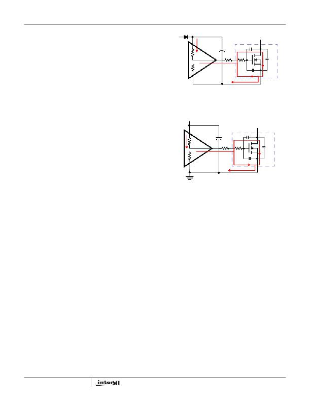
�PHASE�
�FIGURE� 3.� TYPICAL� UPPER-GATE� DRIVE� TURN-ON� PATH�
�Q� G2� ?� PVCC� 2�
�P� Qg_Q2� =� ---------------------------------------� ?� f� SW� ?� N� Q2�
�V� GS2�
�PVCC�
�D�
�I� DR� =� ?� ?� ?� f� SW� +� I� Q�
�?� Q� G1� ?� PVCC� ?� N� Q1� Q� G2� ?� PVCC� ?� N� Q2� ?�
�-----------------------------------------------------� +� -----------------------------------------------------�
�?� V� GS1� V� GS2� ?�
�(EQ.� 3)�
�where� the� gate� charge� (Q� G1� and� Q� G2� )� is� defined� at� a�
�particular� gate� to� source� voltage� (V� GS1� and� V� GS2� )� in� the�
�corresponding� MOSFET� datasheet;� I� Q� is� the� driver� ’s� total�
�R� HI2�
�R� LO2�
�G�
�R� G2�
�C� GD�
�R� GI2�
�C� GS�
�S�
�C� DS�
�Q2�
�quiescent� current� with� no� load� at� both� drive� outputs;� N� Q1�
�and� N� Q2� are� number� of� upper� and� lower� MOSFETs,�
�respectively;� PVCC� is� the� drive� voltage� for� both� upper� and�
�lower� FETs.� The� I� Q*� VCC� product� is� the� quiescent� power� of�
�the� driver� without� capacitive� load� and� is� typically� 116mW� at�
�300kHz� and� VCC� =� PVCC� =� 12V.�
�The� total� gate� drive� power� losses� are� dissipated� among� the�
�resistive� components� along� the� transition� path.� The� drive�
�resistance� dissipates� a� portion� of� the� total� gate� drive� power�
�losses,� the� rest� will� be� dissipated� by� the� external� gate�
�resistors� (R� G1� and� R� G2� )� and� the� internal� gate� resistors�
�(R� GI1� and� R� GI2� )� of� MOSFETs.� Figures� 3� and� 4� show� the�
�typical� upper� and� lower� gate� drives� turn-on� transition� path.�
�The� power� dissipation� on� the� driver� can� be� roughly�
�estimated� as:�
�FIGURE� 4.� TYPICAL� LOWER-GATE� DRIVE� TURN-ON� PATH�
�Application� Information�
�Layout� Considerations�
�The� parasitic� inductances� of� the� PCB� and� of� the� power�
�devices’� packaging� (both� upper� and� lower� MOSFETs)� can�
�cause� serious� ringing,� exceeding� absolute� maximum� rating�
�of� the� devices.� Careful� layout� can� help� minimize� such�
�unwanted� stress.� The� following� advice� is� meant� to� lead� to� an�
�optimized� layout:�
�?� Keep� decoupling� loops� (PVCC-GND� and� BOOT-PHASE)�
�as� short� as� possible.�
�?� Minimize� trace� inductance,� especially� on� low-impedance�
�P� DR_UP� =� ?� --------------------------------------� +� ----------------------------------------� ?� ?� ---------------------�
�?� R� HI1� +� R� EXT1� R� LO1� +� R� EXT1� ?�
�P� DR_LOW� =� ?� --------------------------------------� +� ----------------------------------------� ?� ?� ---------------------�
�?� R� HI2� +� R� EXT2� R� LO2� +� R� EXT2� ?�
�P� DR� =� P� DR_UP� +� P� DR_LOW� +� I� Q� ?� VCC�
�?� R� HI1� R� LO1� ?� P� Qg_Q1�
�?� R� HI2� R� LO2� ?� P� Qg_Q2�
�2�
�2�
�(EQ.� 4)�
�lines.� All� power� traces� (UGATE,� PHASE,� LGATE,� GND,�
�PVCC)� should� be� short� and� wide,� as� much� as� possible.�
�?� Minimize� the� inductance� of� the� PHASE� node.� Ideally,� the�
�source� of� the� upper� and� the� drain� of� the� lower� MOSFET�
�should� be� as� close� as� thermally� allowable.�
�?� Minimize� the� current� loop� of� the� output� and� input� power�
�trains.� Short� the� source� connection� of� the� lower� MOSFET�
�to� ground� as� close� to� the� transistor� pin� as� feasible.� Input�
�R� EXT1� =� R� G1� +� -------------�
�N�
�R� EXT2� =� R� G2� +� -------------�
�N�
�R� GI1�
�Q1�
�8�
�R� GI2�
�Q2�
�capacitors� (especially� ceramic� decoupling)� should� be�
�placed� as� close� to� the� drain� of� upper� and� source� of� lower�
�MOSFETs� as� possible.�
�In� addition,� for� heat� spreading,� place� copper� underneath� the�
�IC� whether� it� has� an� exposed� pad� or� not.� The� copper� area�
�can� be� extended� beyond� the� bottom� area� of� the� IC� and/or�
�connected� to� buried� power� ground� plane(s)� with� thermal�
�FN9282.1�
�December� 3,� 2007�
�相关PDF资料 |
PDF描述 |
|---|---|
| ISL6596IBZ | IC MOSFET DRVR SYNC BUCK 8-SOIC |
| ISL6597CRZ | IC MOSFET DRVR DUAL SYNC 16-QFN |
| ISL6605IBZ | IC DRIVER MOSFET DUAL SYNC 8SOIC |
| ISL6608IR-T | IC MOSFET DRVR SYNC BUCK 8-QFN |
| ISL6609AIRZ-TK | IC MOSFET DVR SYNC RECT 8-QFN |
相关代理商/技术参数 |
参数描述 |
|---|---|
| ISL6594DCRZ-T | 功能描述:IC MOSFET DRVR SYNC BUCK 10-DFN RoHS:是 类别:集成电路 (IC) >> PMIC - MOSFET,电桥驱动器 - 外部开关 系列:- 标准包装:6,000 系列:* |
| ISL6595DRZ | 功能描述:IC DIGITL MULTIPHASE CTRLR 48QFN RoHS:是 类别:集成电路 (IC) >> PMIC - 电源控制器,监视器 系列:- 产品培训模块:Lead (SnPb) Finish for COTS Obsolescence Mitigation Program 标准包装:2,500 系列:- 应用:多相控制器 输入电压:- 电源电压:9 V ~ 14 V 电流 - 电源:- 工作温度:-40°C ~ 85°C 安装类型:表面贴装 封装/外壳:40-WFQFN 裸露焊盘 供应商设备封装:40-TQFN-EP(5x5) 包装:带卷 (TR) |
| ISL6595DRZ-T | 功能描述:IC DIGITL MULTIPHASE CTRLR 48QFN RoHS:是 类别:集成电路 (IC) >> PMIC - 电源控制器,监视器 系列:- 产品培训模块:Lead (SnPb) Finish for COTS Obsolescence Mitigation Program 标准包装:2,500 系列:- 应用:多相控制器 输入电压:- 电源电压:9 V ~ 14 V 电流 - 电源:- 工作温度:-40°C ~ 85°C 安装类型:表面贴装 封装/外壳:40-WFQFN 裸露焊盘 供应商设备封装:40-TQFN-EP(5x5) 包装:带卷 (TR) |
| ISL6595DRZ-TK | 功能描述:IC DIGITL MULTIPHASE CTRLR 48QFN RoHS:是 类别:集成电路 (IC) >> PMIC - 电源控制器,监视器 系列:- 产品培训模块:Lead (SnPb) Finish for COTS Obsolescence Mitigation Program 标准包装:2,500 系列:- 应用:多相控制器 输入电压:- 电源电压:9 V ~ 14 V 电流 - 电源:- 工作温度:-40°C ~ 85°C 安装类型:表面贴装 封装/外壳:40-WFQFN 裸露焊盘 供应商设备封装:40-TQFN-EP(5x5) 包装:带卷 (TR) |
| ISL6595EVAL2 | 制造商:Intersil Corporation 功能描述:DGTL MULTIPHASE CNTRLR - Bulk |
发布紧急采购,3分钟左右您将得到回复。