- 您现在的位置:买卖IC网 > Datasheet目录334 > ISL6608IR-T (Intersil)IC MOSFET DRVR SYNC BUCK 8-QFN Datasheet资料下载
参数资料
| 型号: | ISL6608IR-T |
| 厂商: | Intersil |
| 文件页数: | 9/11页 |
| 文件大小: | 0K |
| 描述: | IC MOSFET DRVR SYNC BUCK 8-QFN |
| 标准包装: | 6,000 |
| 配置: | 高端和低端,同步 |
| 输入类型: | PWM |
| 延迟时间: | 20ns |
| 电流 - 峰: | 2A |
| 配置数: | 1 |
| 输出数: | 2 |
| 电源电压: | 4.5 V ~ 5.5 V |
| 工作温度: | -40°C ~ 85°C |
| 安装类型: | 表面贴装 |
| 封装/外壳: | 8-VQFN 裸露焊盘 |
| 供应商设备封装: | 8-QFN(3x3) |
| 包装: | 带卷 (TR) |
�� �
�
�ISL6608�
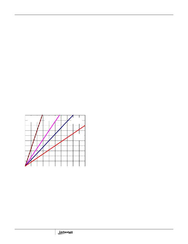
�Power� Dissipation�
�Package� power� dissipation� is� mainly� a� function� of� the�
�switching� frequency� and� total� gate� charge� of� the� selected�
�MOSFETs.� Calculating� the� power� dissipation� in� the� driver� for�
�a� desired� application� is� critical� to� ensuring� safe� operation.�
�Exceeding� the� maximum� allowable� power� dissipation� level�
�will� push� the� IC� beyond� the� maximum� recommended�
�operating� junction� tem� perature� of� 125� °� C.� The� maximum�
�allowable� IC� power� dissipation� for� the� SO-8� package� is�
�approximately� 800mW.� When� designing� the� driver� into� an�
�application,� it� is� recommende� d� that� the� following� calculation�
�be� performed� to� ensure� safe� operation� at� the� desired�
�frequency� for� the� selected� MOSFETs.� The� power� dissipated�
�by� the� driver� is� approximated� as� below� and� plotted� as� in�
�Figure� 9.�
�Layout� Consideration�
�For� heat� spreading,� place� copper� underneath� the� IC� whether�
�it� has� an� exposed� pad� or� not.� The� copper� area� can� be�
�extended� beyond� the� bottom� area� of� the� IC� and/or�
�connected� to� buried� copper� plane(s)� with� thermal� vias.� This�
�combination� of� vias� for� vertical� heat� escape,� extended�
�copper� plane,� and� buried� planes� for� heat� spreading� allows�
�the� IC� to� achieve� its� full� thermal� potential.�
�Place� each� channel� power� component� as� close� to� each�
�other� as� possible� to� reduce� PCB� copper� losses� and� PCB�
�parasitics:� shortest� distance� between� DRAINs� of� upper� FETs�
�and� SOURCEs� of� lower� FETs;� shortest� distance� between�
�DRAINs� of� lower� FETs� and� the� power� ground.� Thus,� smaller�
�amplitudes� of� positive� and� negative� ringing� are� on� the�
�switching� edges� of� the� PHASE� node.� However,� some� space�
�P� =� f� sw� (� 1.5V� U� Q� U� +� V� L� Q� L� )� +� I� DDQ� V�
�CC�
�in� between� power� components� is� required� for� good� airflow.�
�The� gate� traces� from� the� drivers� to� the� FETs� should� be� kept�
�short� and� wide� to� reduce� the� inductance� of� the� traces� and�
�where� f� sw� is� the� switching� frequency� of� the� PWM� signal.� V� U�
�and� V� L� represent� the� upper� and� lower� gate� rail� voltage.� Q� U�
�and� Q� L� are� the� upper� and� lower� gate� charge� determined� by�
�MOSFET� s� election� and� any� external� capacitance� added� to�
�the� gate� pins.� The� I� DDQ� V� CC� product� is� the� quiescent� power�
�of� the� driver� and� is� typically� negligible.�
�promote� clean� drive� signals.�
�1000�
�900�
�Q� U� =100nC�
�Q� L� =200nC�
�Q� U� =50nC�
�Q� L� =100nC�
�Q� U� =50nC�
�Q� L� =50nC�
�800�
�700�
�600�
�500�
�400�
�300�
�200�
�100�
�Q� U� =20nC�
�Q� L� =50nC�
�0�
�0�
�200�
�400�
�600� 800� 1000� 1200� 1400� 1600� 1800� 2000�
�FREQUENCY� (kHz)�
�FIGURE� 9.� POWER� DISSIPATION� vs� FREQUENCY�
�9�
�相关PDF资料 |
PDF描述 |
|---|---|
| ISL6609AIRZ-TK | IC MOSFET DVR SYNC RECT 8-QFN |
| ISL6610IRZ | IC MOSFET DRVR DUAL SYNC 16-QFN |
| ISL6612ACBZ | IC DRIVER MOSFET SYNC BUCK 8SOIC |
| ISL6612BCBZ | IC DRIVER MOSFET SYNC BUCK 8SOIC |
| ISL6613IR-T | IC MOSFET DRVR SYNC BUCK 10-DFN |
相关代理商/技术参数 |
参数描述 |
|---|---|
| ISL6608IRZ | 功能描述:功率驱动器IC VER OF ISL6608IR -40 TO +100 RoHS:否 制造商:Micrel 产品:MOSFET Gate Drivers 类型:Low Cost High or Low Side MOSFET Driver 上升时间: 下降时间: 电源电压-最大:30 V 电源电压-最小:2.75 V 电源电流: 最大功率耗散: 最大工作温度:+ 85 C 安装风格:SMD/SMT 封装 / 箱体:SOIC-8 封装:Tube |
| ISL6608IRZ-T | 功能描述:功率驱动器IC VER OF ISL6608IR-T -40 TO +100 RoHS:否 制造商:Micrel 产品:MOSFET Gate Drivers 类型:Low Cost High or Low Side MOSFET Driver 上升时间: 下降时间: 电源电压-最大:30 V 电源电压-最小:2.75 V 电源电流: 最大功率耗散: 最大工作温度:+ 85 C 安装风格:SMD/SMT 封装 / 箱体:SOIC-8 封装:Tube |
| ISL6609ACBZ | 功能描述:IC MOSFET DRVR SYNC BUCK 8-SOIC RoHS:是 类别:集成电路 (IC) >> PMIC - MOSFET,电桥驱动器 - 外部开关 系列:- 标准包装:50 系列:- 配置:高端 输入类型:非反相 延迟时间:200ns 电流 - 峰:250mA 配置数:1 输出数:1 高端电压 - 最大(自引导启动):600V 电源电压:12 V ~ 20 V 工作温度:-40°C ~ 125°C 安装类型:通孔 封装/外壳:8-DIP(0.300",7.62mm) 供应商设备封装:8-DIP 包装:管件 其它名称:*IR2127 |
| ISL6609ACBZ-T | 功能描述:IC MOSFET DRVR SYNC BUCK 8-SOIC RoHS:是 类别:集成电路 (IC) >> PMIC - MOSFET,电桥驱动器 - 外部开关 系列:- 标准包装:6,000 系列:* |
| ISL6609ACBZ-TS2568 | 制造商:Rochester Electronics LLC 功能描述: 制造商:Intersil Corporation 功能描述: |
发布紧急采购,3分钟左右您将得到回复。