- 您现在的位置:买卖IC网 > PDF目录20572 > ISL6614ACBZ-TR5214 (Intersil)IC DRVR DUAL SYNC BUCK 14-SOIC PDF资料下载
参数资料
| 型号: | ISL6614ACBZ-TR5214 |
| 厂商: | Intersil |
| 文件页数: | 8/12页 |
| 文件大小: | 0K |
| 描述: | IC DRVR DUAL SYNC BUCK 14-SOIC |
| 标准包装: | 2,500 |
| 配置: | 高端和低端,同步 |
| 输入类型: | PWM |
| 延迟时间: | 10ns |
| 电流 - 峰: | 1.25A |
| 配置数: | 2 |
| 输出数: | 4 |
| 高端电压 - 最大(自引导启动): | 36V |
| 电源电压: | 10.8 V ~ 13.2 V |
| 工作温度: | 0°C ~ 85°C |
| 安装类型: | 表面贴装 |
| 封装/外壳: | 14-SOIC(0.154",3.90mm 宽) |
| 供应商设备封装: | 14-SOICN |
| 包装: | 带卷 (TR) |
��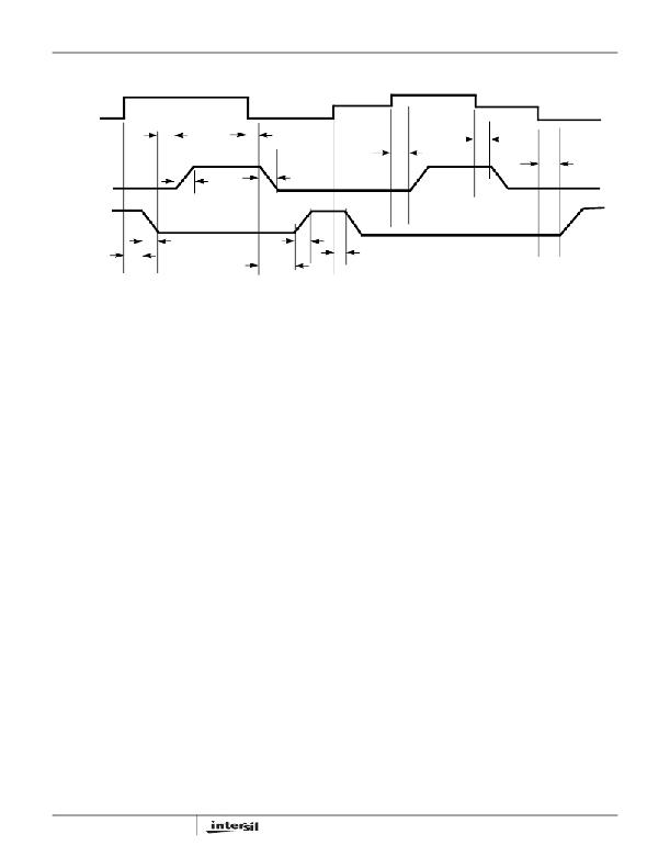 �
�
�ISL6614A�
�Description�
�PWM�
�1.5V<PWM<3.2V�
�1.0V<PWM<2.6V�
�t� PDHU�
�t� PDLU�
�t� PDTS�
�t� TSSHD�
�t� PDTS�
�UGATE�
�LGATE�
�t� PDLL�
�t� FL�
�t� RU�
�t� RL�
�t� FU�
�t� TSSHD�
�t� PDHL�
�FIGURE� 1.� TIMING� DIAGRAM�
�Operation�
�Designed� for� versatility� and� speed,� the� ISL6614A� MOSFET�
�driver� controls� both� high-side� and� low-side� N-Channel� FETs� of�
�two� half-bridge� power� trains� from� two� externally� provided� PWM�
�signals.�
�Prior� to� VCC� exceeding� its� POR� level,� the� Pre-POR�
�overvoltage� protection� function� is� activated� during� initial� startup;�
�the� upper� gate� (UGATE)� is� held� low� and� the� lower� gate�
�(LGATE),� controlled� by� the� Pre-POR� overvoltage� protection�
�circuits,� is� connected� to� the� PHASE.� Once� the� VCC� voltage�
�surpasses� the� VCC� Rising� Threshold� (See� “Electrical�
�Specifications”� table� on� page� 5),� the� PWM� signal� takes� control�
�of� gate� transitions.� A� rising� edge� on� PWM� initiates� the� turn-off� of�
�the� lower� MOSFET� (see� “TIMING� DIAGRAM”� on� page� 8).� After�
�a� short� propagation� delay� [t� PDLL� ],� the� lower� gate� begins� to� fall.�
�Typical� fall� times� [t� FL� ]� are� provided� in� the� “Electrical�
�Specifications”� table� on� page� 6.� Adaptive� shoot-through�
�circuitry� monitors� the� PHASE� voltage� and� determines� the� upper�
�gate� delay� time� [t� PDHU� ].� This� prevents� both� the� lower� and�
�upper� MOSFETs� from� conducting� simultaneously.� Once� this�
�delay� period� is� complete,� the� upper� gate� drive� begins� to� rise�
�[t� RU� ]� and� the� upper� MOSFET� turns� on.�
�A� falling� transition� on� PWM� results� in� the� turn-off� of� the� upper�
�MOSFET� and� the� turn-on� of� the� lower� MOSFET.� A� short�
�propagation� delay� [t� PDLU� ]� is� encountered� before� the� upper�
�gate� begins� to� fall� [t� FU� ].� Again,� the� adaptive� shoot-through�
�circuitry� determines� the� lower� gate� delay� time,� t� PDHL� .� The�
�PHASE� voltage� and� the� UGATE� voltage� are� monitored,� and�
�the� lower� gate� is� allowed� to� rise� after� PHASE� drops� below� a�
�level� or� the� voltage� of� UGATE� to� PHASE� reaches� a� level�
�depending� upon� the� current� direction� (See� the� following�
�section� for� details).� The� lower� gate� then� rises� [t� RL� ],� turning� on�
�the� lower� MOSFET.�
�8�
�Advanced� Adaptive� Zero� Shoot-Through� Deadtime�
�Control� (Patent� Pending)�
�These� drivers� incorporate� a� unique� adaptive� deadtime� control�
�technique� to� minimize� deadtime,� resulting� in� high� efficiency�
�from� the� reduced� freewheeling� time� of� the� lower� MOSFETs’�
�body-diode� conduction,� and� to� prevent� the� upper� and� lower�
�MOSFETs� from� conducting� simultaneously.� This� is�
�accomplished� by� ensuring� either� rising� gate� turns� on� its�
�MOSFET� with� minimum� and� sufficient� delay� after� the� other� has�
�turned� off.�
�During� turn-off� of� the� lower� MOSFET,� the� PHASE� voltage� is�
�monitored� until� it� reaches� a� -0.2V/+0.8V� trip� point� for� a�
�forward/reverse� current,� at� which� time� the� UGATE� is� released�
�to� rise.� An� auto-zero� comparator� is� used� to� correct� the�
�r� DS(ON)� drop� in� the� phase� voltage� preventing� from� false�
�detection� of� the� -0.2V� phase� level� during� r� DS(ON)� conduction�
�period.� In� the� case� of� zero� current,� the� UGATE� is� released�
�after� 35ns� delay� of� the� LGATE� dropping� below� 0.5V.� During�
�the� phase� detection,� the� disturbance� of� LGATE’s� falling�
�transition� on� the� PHASE� node� is� blanked� out� to� prevent� falsely�
�tripping.� Once� the� PHASE� is� high,� the� advanced� adaptive�
�shoot-through� circuitry� monitors� the� PHASE� and� UGATE�
�voltages� during� a� PWM� falling� edge� and� the� subsequent�
�UGATE� turn-off.� If� either� the� UGATE� falls� to� less� than� 1.75V�
�above� the� PHASE� or� the� PHASE� falls� to� less� than� +0.8V,� the�
�LGATE� is� released� to� turn� on.�
�Three-State� PWM� Input�
�A� unique� feature� of� these� drivers� and� other� Intersil� drivers� is�
�the� addition� of� a� shutdown� window� to� the� PWM� input.� If� the�
�PWM� signal� enters� and� remains� within� the� shutdown� window�
�for� a� set� holdoff� time,� the� driver� outputs� are� disabled� and�
�both� MOSFET� gates� are� pulled� and� held� low.� The� shutdown�
�state� is� removed� when� the� PWM� signal� moves� outside� the�
�shutdown� window.� Otherwise,� the� PWM� rising� and� falling�
�thresholds� outlined� in� the� “Electrical� Specifications”� table� on�
�FN9160.4�
�May� 5,� 2008�
�相关PDF资料 |
PDF描述 |
|---|---|
| ISL6614CBZR5238 | IC DRVR DUAL SYNC BUCK 14-SOIC |
| VI-BV0-CY-B1 | CONVERTER MOD DC/DC 5V 50W |
| ISL6614CBZA-T | IC DRIVER DUAL SYNC BUCK 14-SOIC |
| VI-B5K-CY-B1 | CONVERTER MOD DC/DC 40V 50W |
| VI-B5H-CY-B1 | CONVERTER MOD DC/DC 52V 50W |
相关代理商/技术参数 |
参数描述 |
|---|---|
| ISL6614ACR | 功能描述:IC DRIVER MOSFET DUAL SYNC 16QFN RoHS:否 类别:集成电路 (IC) >> PMIC - MOSFET,电桥驱动器 - 外部开关 系列:- 标准包装:50 系列:- 配置:低端 输入类型:非反相 延迟时间:40ns 电流 - 峰:9A 配置数:1 输出数:1 高端电压 - 最大(自引导启动):- 电源电压:4.5 V ~ 35 V 工作温度:-40°C ~ 125°C 安装类型:表面贴装 封装/外壳:TO-263-6,D²Pak(5 引线+接片),TO-263BA 供应商设备封装:TO-263 包装:管件 |
| ISL6614ACR-T | 功能描述:IC DRIVER DUAL SYNC BUCK 16-QFN RoHS:否 类别:集成电路 (IC) >> PMIC - MOSFET,电桥驱动器 - 外部开关 系列:- 标准包装:50 系列:- 配置:低端 输入类型:非反相 延迟时间:40ns 电流 - 峰:9A 配置数:1 输出数:1 高端电压 - 最大(自引导启动):- 电源电压:4.5 V ~ 35 V 工作温度:-40°C ~ 125°C 安装类型:表面贴装 封装/外壳:TO-263-6,D²Pak(5 引线+接片),TO-263BA 供应商设备封装:TO-263 包装:管件 |
| ISL6614ACRZ | 功能描述:IC DRIVER DUAL SYNC BUCK 16-QFN RoHS:是 类别:集成电路 (IC) >> PMIC - MOSFET,电桥驱动器 - 外部开关 系列:- 标准包装:50 系列:- 配置:高端 输入类型:非反相 延迟时间:200ns 电流 - 峰:250mA 配置数:1 输出数:1 高端电压 - 最大(自引导启动):600V 电源电压:12 V ~ 20 V 工作温度:-40°C ~ 125°C 安装类型:通孔 封装/外壳:8-DIP(0.300",7.62mm) 供应商设备封装:8-DIP 包装:管件 其它名称:*IR2127 |
| ISL6614ACRZ-T | 功能描述:IC DRIVER DUAL SYNC BUCK 16-QFN RoHS:是 类别:集成电路 (IC) >> PMIC - MOSFET,电桥驱动器 - 外部开关 系列:- 标准包装:50 系列:- 配置:高端 输入类型:非反相 延迟时间:200ns 电流 - 峰:250mA 配置数:1 输出数:1 高端电压 - 最大(自引导启动):600V 电源电压:12 V ~ 20 V 工作温度:-40°C ~ 125°C 安装类型:通孔 封装/外壳:8-DIP(0.300",7.62mm) 供应商设备封装:8-DIP 包装:管件 其它名称:*IR2127 |
| ISL6614AIB | 功能描述:IC DRIVER MOSF DUAL SYNC 14SOIC RoHS:否 类别:集成电路 (IC) >> PMIC - MOSFET,电桥驱动器 - 外部开关 系列:- 标准包装:50 系列:- 配置:低端 输入类型:非反相 延迟时间:40ns 电流 - 峰:9A 配置数:1 输出数:1 高端电压 - 最大(自引导启动):- 电源电压:4.5 V ~ 35 V 工作温度:-40°C ~ 125°C 安装类型:表面贴装 封装/外壳:TO-263-6,D²Pak(5 引线+接片),TO-263BA 供应商设备封装:TO-263 包装:管件 |
发布紧急采购,3分钟左右您将得到回复。