- 您现在的位置:买卖IC网 > PDF目录20546 > ISL6614BCBZ (Intersil)IC DRVR DUAL SYNC BUCK 14-SOIC PDF资料下载
参数资料
| 型号: | ISL6614BCBZ |
| 厂商: | Intersil |
| 文件页数: | 8/11页 |
| 文件大小: | 0K |
| 描述: | IC DRVR DUAL SYNC BUCK 14-SOIC |
| 标准包装: | 1,000 |
| 配置: | 高端和低端,同步 |
| 输入类型: | PWM |
| 延迟时间: | 10ns |
| 电流 - 峰: | 1.25A |
| 配置数: | 2 |
| 输出数: | 4 |
| 高端电压 - 最大(自引导启动): | 36V |
| 电源电压: | 7 V ~ 13.2 V |
| 工作温度: | 0°C ~ 85°C |
| 安装类型: | 表面贴装 |
| 封装/外壳: | 14-SOIC(0.154",3.90mm 宽) |
| 供应商设备封装: | 14-SOICN |
| 包装: | 管件 |
�� �
�
�ISL6614B�
�on� page� 5� determine� when� the� lower� and� upper� gates� are�
�enabled.�
�This� feature� helps� prevent� a� negative� transient� on� the� output�
�voltage� when� the� output� is� shut� down,� eliminating� the�
�Schottky� diode� that� is� used� in� some� systems� for� protecting�
�the� load� from� reversed� output� voltage� events.�
�In� addition,� more� than� 400mV� hysteresis� also� incorporates�
�into� the� three-state� shutdown� window� to� eliminate� PWM�
�input� oscillations� due� to� the� capacitive� load� seen� by� the�
�PWM� input� through� the� body� diode� of� the� controller� ’s� PWM�
�output� when� the� power-up� and/or� power-down� sequence� of�
�bias� supplies� of� the� driver� and� PWM� controller� are� required.�
�where� Q� G1� is� the� amount� of� gate� charge� per� upper� MOSFET�
�at� V� GS1� gate-source� voltage� and� N� Q1� is� the� number� of�
�control� MOSFETs� per� channel.� The� Δ� V� BOOT_CAP� term� is�
�defined� as� the� allowable� droop� in� the� rail� of� the� upper� gate�
�drive.�
�As� an� example,� suppose� two� IRLR7821� FETs� are� chosen� as�
�the� upper� MOSFETs.� The� gate� charge,� Q� G� ,� from� the� data�
�sheet� is� 10nC� at� 4.5V� (V� GS� )� gate-source� voltage.� Then� the�
�Q� GATE� is� calculated� to� be� 53nC� for� PVCC� =� 12V.� We� will�
�assume� a� 200mV� droop� in� drive� voltage� over� the� PWM�
�cycle.� We� find� that� a� bootstrap� capacitance� of� at� least�
�0.267μF� is� required.�
�1.6�
�Power-On� Reset� (POR)� Function�
�During� initial� startup,� the� VCC� voltage� rise� is� monitored.�
�Once� the� rising� VCC� voltage� exceeds� 6.9V� (typically),�
�operation� of� the� driver� is� enabled� and� the� PWM� input� signal�
�takes� control� of� the� gate� drives.� If� VCC� drops� below� the�
�falling� threshold� of� 5.6V� (typically),� operation� of� the� driver� is�
�disabled.�
�Pre-POR� Overvoltage� Protection�
�1.4�
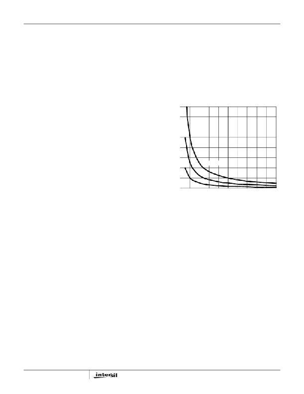
�1.2�
�1.0�
�0.8�
�0.6�
�Prior� to� VCC� exceeding� its� POR� level,� the� upper� gate� is� held�
�low� and� the� lower� gate� is� controlled� by� the� overvoltage�
�protection� circuits� during� initial� startup.� The� PHASE� is�
�connected� to� the� gate� of� the� low� side� MOSFET� (LGATE),�
�0.4�
�0.2�
�20nC�
�Q� GATE� = 100nC�
�50nC�
�which� provides� some� protection� to� the� microprocessor� if� the�
�0.0�
�0.0�
�0.1�
�0.2�
�0.3�
�0.4�
�0.5�
�0.6�
�0.7�
�0.8�
�0.9�
�1.0�
�upper� MOSFET(s)� is� shorted� during� initial� start-up.� For�
�complete� protection,� the� low� side� MOSFET� should� have� a�
�gate� threshold� well� below� the� maximum� voltage� rating� of� the�
�load/microprocessor.�
�When� VCC� drops� below� its� POR� level,� both� gates� pull� low�
�and� the� Pre-POR� overvoltage� protection� circuits� are� not�
�activated� until� VCC� resets.�
�Internal� Bootstrap� Device�
�Both� drivers� feature� an� internal� bootstrap� schottky� diode.�
�Simply� adding� an� external� capacitor� across� the� BOOT� and�
�PHASE� pins� completes� the� bootstrap� circuit.� The� bootstrap�
�function� is� also� designed� to� prevent� the� bootstrap� capacitor�
�from� overcharging� due� to� the� large� negative� swing� at� the�
�trailing-edge� of� the� PHASE� node.� This� reduces� voltage�
�stress� on� the� boot� to� phase� pins.�
�The� bootstrap� capacitor� must� have� a� maximum� voltage�
�rating� above� UVCC� +� 5V� and� its� capacitance� value� can� be�
�chosen� from� Equation� 1:�
�Δ� V� BOOT_CAP� (V)�
�FIGURE� 2.� BOOTSTRAP� CAPACITANCE� vs� BOOT� RIPPLE�
�VOLTAGE�
�Gate� Drive� Voltage� Versatility�
�The� ISL6614B� provides� the� user� flexibility� in� choosing� the�
�gate� drive� voltage� for� efficiency� optimization.� The� ISL6614B�
�ties� the� upper� and� lower� drive� rails� together.� Simply� applying�
�a� voltage� from� 5V� up� to� 12V� on� PVCC� sets� both� gate� drive�
�rail� voltages� simultaneously.� Connecting� a� SOT-23� package�
�type� of� dual� Schottky� diodes� from� the� VCC� to� BOOT1� and�
�BOOT2� can� bypass� the� internal� bootstrap� devices� of� both�
�upper� gates� so� that� the� part� can� operate� as� a� dual� ISL6612B�
�driver,� which� has� a� fixed� VCC� (7V� to� 12V� typically)� on� the�
�upper� gate� and� a� programmable� lower� gate� drive� voltage.�
�Power� Dissipation�
�Package� power� dissipation� is� mainly� a� function� of� the�
�switching� frequency� (f� SW� ),� the� output� drive� impedance,� the�
�C� BOOT_CAP� ≥� --------------------------------------�
�Q� GATE� =� ------------------------------------� ?� N� Q1�
�Q� GATE�
�Δ� V� BOOT_CAP�
�Q� G1� ?� PVCC�
�V� GS1�
�8�
�(EQ.� 1)�
�external� gate� resistance,� and� the� selected� MOSFET’s�
�internal� gate� resistance� and� total� gate� charge.� Calculating�
�the� power� dissipation� in� the� driver� for� a� desired� application� is�
�critical� to� ensure� safe� operation.� Exceeding� the� maximum�
�allowable� power� dissipation� level� will� push� the� IC� beyond� the�
�maximum� recommended� operating� junction� temperature� of�
�+125°C.� The� maximum� allowable� IC� power� dissipation� for�
�the� SO14� package� is� approximately� 1W� at� room�
�temperature,� while� the� power� dissipation� capacity� in� the�
�FN9206.3�
�May� 5,� 2008�
�相关PDF资料 |
PDF描述 |
|---|---|
| RACD06-350 | LED DRIVER 6W 3-21V OUT LED DR |
| 396-056-526-201 | CARD EDGE 56POS DL .125X.250 BLK |
| T95V685K010HSAL | CAP TANT 6.8UF 10V 10% 1410 |
| 396-056-522-804 | CARD EDGE 56POS DL .125X.250 BLK |
| AT45DB161B-TC-2.5 | IC FLASH 16MBIT 20MHZ 28TSOP |
相关代理商/技术参数 |
参数描述 |
|---|---|
| ISL6614BCBZ-T | 功能描述:IC DRVR DUAL SYNC BUCK 14-SOIC RoHS:是 类别:集成电路 (IC) >> PMIC - MOSFET,电桥驱动器 - 外部开关 系列:- 标准包装:50 系列:- 配置:高端 输入类型:非反相 延迟时间:200ns 电流 - 峰:250mA 配置数:1 输出数:1 高端电压 - 最大(自引导启动):600V 电源电压:12 V ~ 20 V 工作温度:-40°C ~ 125°C 安装类型:通孔 封装/外壳:8-DIP(0.300",7.62mm) 供应商设备封装:8-DIP 包装:管件 其它名称:*IR2127 |
| ISL6614BCRZ | 功能描述:IC DRVR DUAL SYNC BUCK 16-QFN RoHS:是 类别:集成电路 (IC) >> PMIC - MOSFET,电桥驱动器 - 外部开关 系列:- 标准包装:50 系列:- 配置:高端 输入类型:非反相 延迟时间:200ns 电流 - 峰:250mA 配置数:1 输出数:1 高端电压 - 最大(自引导启动):600V 电源电压:12 V ~ 20 V 工作温度:-40°C ~ 125°C 安装类型:通孔 封装/外壳:8-DIP(0.300",7.62mm) 供应商设备封装:8-DIP 包装:管件 其它名称:*IR2127 |
| ISL6614BCRZ-T | 功能描述:IC DRVR DUAL SYNC BUCK 16-QFN RoHS:是 类别:集成电路 (IC) >> PMIC - MOSFET,电桥驱动器 - 外部开关 系列:- 标准包装:50 系列:- 配置:高端 输入类型:非反相 延迟时间:200ns 电流 - 峰:250mA 配置数:1 输出数:1 高端电压 - 最大(自引导启动):600V 电源电压:12 V ~ 20 V 工作温度:-40°C ~ 125°C 安装类型:通孔 封装/外壳:8-DIP(0.300",7.62mm) 供应商设备封装:8-DIP 包装:管件 其它名称:*IR2127 |
| ISL6614BIBZ | 功能描述:IC DRVR DUAL SYNC BUCK 14-SOIC RoHS:是 类别:集成电路 (IC) >> PMIC - MOSFET,电桥驱动器 - 外部开关 系列:- 标准包装:50 系列:- 配置:高端 输入类型:非反相 延迟时间:200ns 电流 - 峰:250mA 配置数:1 输出数:1 高端电压 - 最大(自引导启动):600V 电源电压:12 V ~ 20 V 工作温度:-40°C ~ 125°C 安装类型:通孔 封装/外壳:8-DIP(0.300",7.62mm) 供应商设备封装:8-DIP 包装:管件 其它名称:*IR2127 |
| ISL6614BIBZ-T | 功能描述:IC DRVR DUAL SYNC BUCK 14-SOIC RoHS:是 类别:集成电路 (IC) >> PMIC - MOSFET,电桥驱动器 - 外部开关 系列:- 标准包装:50 系列:- 配置:高端 输入类型:非反相 延迟时间:200ns 电流 - 峰:250mA 配置数:1 输出数:1 高端电压 - 最大(自引导启动):600V 电源电压:12 V ~ 20 V 工作温度:-40°C ~ 125°C 安装类型:通孔 封装/外壳:8-DIP(0.300",7.62mm) 供应商设备封装:8-DIP 包装:管件 其它名称:*IR2127 |
发布紧急采购,3分钟左右您将得到回复。