参数资料
| 型号: | ISL6700EVAL1Z |
| 厂商: | Intersil |
| 文件页数: | 4/8页 |
| 文件大小: | 0K |
| 描述: | EVALUATION BOARD FOR ISL6700 |
| 标准包装: | 1 |
| 系列: | * |
�� �
�
�ISL6700�
�Absolute� Maximum� Ratings�
�Supply� Voltage,� V� DD� (Note� 1)� .� .� .� .� .� .� .� .� .� .� .� .� .� .� .� .� .� .� .� -0.3V� to� 16V�
�LI� and� HI� Voltages� (Note� 1)� .� .� .� .� .� .� .� .� .� .� .� .� .� .� .� .� -0.3V� to� V� DD� +0.3V�
�Voltage� on� HS� (Note� 1)� .� .� .� .� .� .� .� .� .� .� .� .� .� .� .� .� .� .� .� .� .� .� .� .� .� .� 0V� to� 80V�
�Voltage� on� HB� (Note� 1)� .� .� .� .� .� .� .� .� .� .� .� .� .� .� .� .� V� HS� -0.3V� to� V� HS� +V� DD�
�Voltage� on� LO� (Note� 1)� .� .� .� .� .� .� .� .� .� .� .� .� .� .� .� .� .� V� SS� -0.3� to� V� DD� +0.3V�
�Voltage� on� HO� (Note� 1)� .� .� .� .� .� .� .� .� .� .� .� .� .� .� .� .� V� HS� -0.3V� to� V� HB� +0.3V�
�Phase� Slew� Rate� .� .� .� .� .� .� .� .� .� .� .� .� .� .� .� .� .� .� .� .� .� .� .� .� .� .� .� .� .� .� .� .� .� .� 20V/ns�
�Maximum� Recommended� Operating� Conditions�
�Supply� Voltage,� V� DD� .� .� .� .� .� .� .� .� .� .� .� .� .� .� .� .� .� .� .� .� .� .� .� .� .� .� .� .� .� 9V� to� 15V�
�Voltage� on� HS� .� .� .� .� .� .� .� .� .� .� .� .� .� .� .� .� .� .� .� .� .� .� .� .� .� .� .� .� .� .� .� .� .� .� 0V� to� 75V�
�Thermal� Information�
�Thermal� Resistance� (Typical)� θ� JA� (°C/W)� θ� JC� (°C/W)�
�SOIC� (Note� 3)� .� .� .� .� .� .� .� .� .� .� .� .� .� .� .� .� .� .� .� 95� N/A�
�QFN� (Note� 4)� .� .� .� .� .� .� .� .� .� .� .� .� .� .� .� .� .� .� .� .� 49� 7�
�Max� Power� Dissipation� at� 25°C� in� Free� Air� (SOIC,� Note� 3).� 1.316W�
�Max� Power� Dissipation� at� 25°C� in� Free� Air� (QFN,� Note� 4)� .� .2.976W�
�Maximum� Storage� Temperature� Range� .� .� .� .� .� .� .� .� .� .-65°C� to� +150°C�
�Maximum� Junction� Temperature� Range� .� .� .� .� .� .� .� .� .-40°C� to� +150°C�
�Maximum� Lead� Temperature� (Soldering� 10s)� .� .� .� .� .� .� .� .� .� .� .� +300°C�
�(SOIC� -� Lead� Tips� Only)�
�For� Recommended� soldering� conditions� see� Tech� Brief� TB389.�
�Voltage� on� HS� (Note� 2)� .� .� .� .� .� .� .� .� .� .(Repetitive� Transient)� -1V� to� 80V�
�Voltage� on� HB� .� .� .� .� .� .� .� .� .� .� .� .� .� .� .� .� .� .� .� .� .� .� .� .� .� .� V� HS� +7.5V� to� V� HS� +V� DD�
�CAUTION:� Stresses� above� those� listed� in� “Absolute� Maximum� Ratings”� may� cause� permanent� damage� to� the� device.� This� is� a� stress� only� rating� and� operation� of� the�
�device� at� these� or� any� other� conditions� above� those� indicated� in� the� recommended� operating� conditions� of� this� specification� is� not� implied.�
�NOTES:�
�1.� All� voltages� referenced� to� V� SS� unless� otherwise� specified.�
�2.� Based� on� V� DD� =15V.� The� magnitude� of� the� allowable� negative� transient� on� the� HS� pin� is� a� function� of� the� V� DD� supply� voltage.� V� HS� <15.6V-�
�V� DD� +V� F� ,� where� V� HS� is� the� magnitude� of� the� allowable� negative� transient� and� V� F� is� the� forward� voltage� drop� of� the� bootstrap� diode.�
�3.� θ� JA� is� measured� with� the� component� mounted� on� a� high� effective� thermal� conductivity� test� board� in� free� air.� See� Tech� Brief� TB379� for� details.�
�4.� θ� JA� is� measured� in� free� air� with� the� component� mounted� on� a� high� effective� thermal� conductivity� test� board� with� “direct� attach”� features.� θ� JC� ,� the�
�“case� temp”� is� measured� at� the� center� of� the� exposed� metal� pad� on� the� package� underside.� See� Tech� Brief� TB379.�
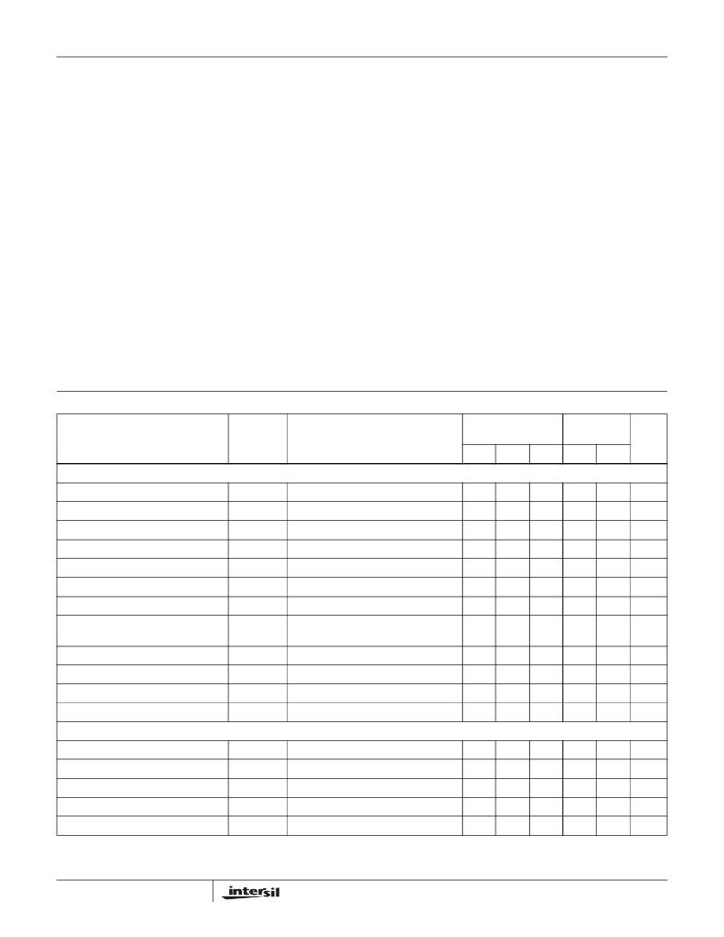
�Electrical� Specifications�
�V� DD� =� V� HB� =� 12V,� V� SS� =� V� HS� =� 0V,� No� Load� on� LO� or� HO,� Unless� Otherwise� Specified�
�T� J� =� 25°C�
�T� J� =� -40°C� TO�
�125°C�
�PARAMETERS�
�SYMBOL�
�TEST� CONDITIONS�
�MIN�
�TYP�
�MAX�
�MIN�
�MAX�
�UNITS�
�SUPPLY� CURRENTS� &� UNDERVOLTAGE� PROTECTION�
�V� DD� Quiescent� Current�
�V� DD� Operating� Current�
�V� DD� Operating� Current�
�HB� Off� Quiescent� Current�
�HB� On� Quiescent� Current�
�HB� Operating� Current�
�HB� Operating� Current�
�HS� Leakage� Current�
�V� DD� Rising� Undervoltage� Threshold�
�V� DD� Falling� Undervoltage� Threshold�
�Undervoltage� Hysteresis�
�HB� Undervoltage� Threshold�
�I� DD�
�I� DDO�
�I� DDO�
�I� HBL�
�I� HBH�
�I� HBO�
�I� HBO�
�I� HLK�
�V� DDUV+�
�V� DDUV-�
�UVHYS�
�VHBUV�
�LI� =� 0� or� V� DD�
�f� =� 50kHz�
�f� =� 500kHz�
�HI� =� 0�
�HI� =� V� DD�
�f� =� 50kHz,� C� L� =� 1000pF�
�f� =� 500kHz,� C� L� =� 1000pF�
�V� HS� =� 80V�
�V� HB� =� 96V�
�Referenced� to� HS�
�-�
�-�
�-�
�-�
�-�
�-�
�-�
�-�
�6.8�
�6.5�
�0.17�
�4.8�
�1.9�
�2.0�
�2.5�
�1.25�
�170�
�1.45�
�2.4�
�-�
�7.6�
�7.1�
�0.45�
�5.3�
�2.2�
�2.2�
�3.0�
�1.5�
�240�
�1.8�
�2.8�
�1�
�8.25�
�7.8�
�0.75�
�6.5�
�-�
�-�
�-�
�-�
�-�
�-�
�-�
�-�
�6.5�
�6.25�
�0.15�
�4.0�
�2.4�
�2.5�
�4.0�
�1.8�
�250�
�2.0�
�3.0�
�1�
�8.5�
�8.1�
�0.90�
�7.5�
�mA�
�mA�
�mA�
�mA�
�μ� A�
�mA�
�mA�
�μ� A�
�V�
�V�
�V�
�V�
�INPUT� PINS:� LI� and� HI�
�Low� Level� Input� Voltage�
�High� Level� Input� Voltage�
�Input� Voltage� Hysteresis�
�Low� Level� Input� Current�
�High� Level� Input� Current�
�V� IL�
�V� IH�
�I� IL�
�I� IH�
�Full� Operating� Conditions�
�Full� Operating� Conditions�
�V� IN� =� 0V,� Full� Operating� Conditions�
�V� IN� =� 5V,� Full� Operating� Conditions�
�0.8�
�-�
�-�
�-70�
�30�
�1.6�
�1.7�
�100�
�-60�
�115�
�-�
�2.2�
�-�
�-30�
�130�
�0.8�
�-�
�-�
�-80�
�30�
�-�
�2.2�
�-�
�-30�
�145�
�V�
�V�
�mV�
�μ� A�
�μ� A�
�4�
�FN9077.6�
�December� 29,� 2004�
�相关PDF资料 |
PDF描述 |
|---|---|
| ISL6844EVAL1 | EVALUATION BOARD 1 ISL6844 |
| ISL6AHPEVAL1 | EVAL BOARD HIP1011D/ISL6118 |
| ISL70218SRHMEVAL1Z | EVALUATION BOARD FOR ISL70218SRH |
| ISL8107EVAL1Z | EVAL BOARD FOR ISL8107 |
| ISL88550AEVAL1 | EVALUATION BOARD 1 ISL88550A |
相关代理商/技术参数 |
参数描述 |
|---|---|
| ISL6700IB | 功能描述:IC DRIVER HALF BRIDGE DUAL 8SOIC RoHS:否 类别:集成电路 (IC) >> PMIC - MOSFET,电桥驱动器 - 外部开关 系列:- 标准包装:50 系列:- 配置:低端 输入类型:非反相 延迟时间:40ns 电流 - 峰:9A 配置数:1 输出数:1 高端电压 - 最大(自引导启动):- 电源电压:4.5 V ~ 35 V 工作温度:-40°C ~ 125°C 安装类型:表面贴装 封装/外壳:TO-263-6,D²Pak(5 引线+接片),TO-263BA 供应商设备封装:TO-263 包装:管件 |
| ISL6700IB-T | 功能描述:IC DRIVER HALF BRIDGE TTL 8-SOIC RoHS:否 类别:集成电路 (IC) >> PMIC - MOSFET,电桥驱动器 - 外部开关 系列:- 标准包装:50 系列:- 配置:低端 输入类型:非反相 延迟时间:40ns 电流 - 峰:9A 配置数:1 输出数:1 高端电压 - 最大(自引导启动):- 电源电压:4.5 V ~ 35 V 工作温度:-40°C ~ 125°C 安装类型:表面贴装 封装/外壳:TO-263-6,D²Pak(5 引线+接片),TO-263BA 供应商设备封装:TO-263 包装:管件 |
| ISL6700IBZ | 功能描述:功率驱动器IC 75V/1 25A PEAK H-BRDG DRVR RoHS:否 制造商:Micrel 产品:MOSFET Gate Drivers 类型:Low Cost High or Low Side MOSFET Driver 上升时间: 下降时间: 电源电压-最大:30 V 电源电压-最小:2.75 V 电源电流: 最大功率耗散: 最大工作温度:+ 85 C 安装风格:SMD/SMT 封装 / 箱体:SOIC-8 封装:Tube |
| ISL6700IBZ-T | 功能描述:功率驱动器IC 75V 1.25A PEAK HALF BRDG DRVR RoHS:否 制造商:Micrel 产品:MOSFET Gate Drivers 类型:Low Cost High or Low Side MOSFET Driver 上升时间: 下降时间: 电源电压-最大:30 V 电源电压-最小:2.75 V 电源电流: 最大功率耗散: 最大工作温度:+ 85 C 安装风格:SMD/SMT 封装 / 箱体:SOIC-8 封装:Tube |
| ISL6700IR | 功能描述:功率驱动器IC HALF BRIDGE DUAL RoHS:否 制造商:Micrel 产品:MOSFET Gate Drivers 类型:Low Cost High or Low Side MOSFET Driver 上升时间: 下降时间: 电源电压-最大:30 V 电源电压-最小:2.75 V 电源电流: 最大功率耗散: 最大工作温度:+ 85 C 安装风格:SMD/SMT 封装 / 箱体:SOIC-8 封装:Tube |
发布紧急采购,3分钟左右您将得到回复。