- 您现在的位置:买卖IC网 > PDF目录15060 > ISL6729IU (Intersil)IC REG CTRLR BST FLYBK ISO 8MSOP PDF资料下载
参数资料
| 型号: | ISL6729IU |
| 厂商: | Intersil |
| 文件页数: | 5/8页 |
| 文件大小: | 0K |
| 描述: | IC REG CTRLR BST FLYBK ISO 8MSOP |
| 标准包装: | 98 |
| PWM 型: | 电流模式 |
| 输出数: | 1 |
| 频率 - 最大: | 2MHz |
| 占空比: | 100% |
| 电源电压: | 4.75 V ~ 5.25 V |
| 降压: | 是 |
| 升压: | 是 |
| 回扫: | 是 |
| 反相: | 无 |
| 倍增器: | 无 |
| 除法器: | 无 |
| Cuk: | 无 |
| 隔离: | 是 |
| 工作温度: | -40°C ~ 105°C |
| 封装/外壳: | 8-TSSOP,8-MSOP(0.118",3.00mm 宽) |
| 包装: | 管件 |
�� �
�
�ISL6729�
�Electrical� Specifications�
�Recommended� operating� conditions� unless� otherwise� noted.� Refer� to� Block� Diagram� and� Typical� Application�
�schematic.� V� DD� =� 5V,� CLK� =� 50kHz,� T� A� =� -40� to� 105°C� (Note� 3),� Typical� values� are� at� T� A� =� 25°C� (Continued)�
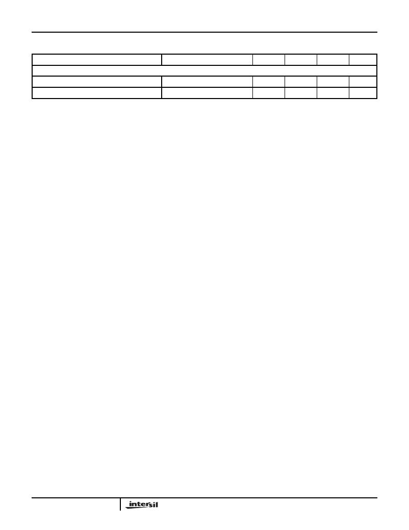
�PARAMETER�
�TEST� CONDITIONS�
�MIN�
�TYP�
�MAX�
�UNITS�
�PWM�
�Maximum� Duty� Cycle�
�Minimum� Duty� Cycle�
�-�
�-�
�99�
�-�
�-�
�0�
�%�
�%�
�NOTES:�
�3.� Specifications� at� -40°C� are� guaranteed� by� design,� not� production� tested.�
�4.� This� is� the� V� DD� current� consumed� when� the� device� is� active� but� not� switching.� Does� not� include� gate� drive� current.�
�5.� Guaranteed� by� design,� not� 100%� tested� in� production.�
�Pin� Descriptions�
�CLK� -� This� is� the� oscillator� timing� control� pin.� The�
�operational� frequency� and� maximum� duty� cycle� are� set� by�
�applying� a� 5V� amplitude� clock� signal� to� CLK.� The� logic� high�
�duration� defines� the� maximum� ON� time� for� the� output.� A�
�maximum� clock� rate� up� to� 2.0MHz� is� possible.�
�COMP� -� COMP� is� the� input� to� the� PWM� comparator� and� is�
�typically� controlled� through� an� external� error� amplifier.�
�CS� -� This� is� the� current� sense� input� to� the� PWM� comparator.�
�The� range� of� the� input� signal� is� nominally� 0� to� 1.0V� and� has�
�an� internal� offset� of� 100mV.�
�GND� -� GND� is� the� power� and� small� signal� reference� ground�
�for� all� functions.�
�OUT� -� This� is� the� drive� output� to� the� power� switching� device.�
�It� is� a� high� current� output� capable� of� driving� the� gate� of� a�
�power� MOSFET� with� peak� currents� of� 1.0A� .� This� GATE�
�output� is� actively� held� low� when� V� DD� is� below� the� UVLO�
�threshold.�
�V� DD� -� V� DD� is� the� 5V� power� connection� for� the� IC.� The� IC� will�
�operate� from� 4.75V� to� 5.25V.� However,� the� accuracy� of� the�
�voltage� clamp� on� the� COMP� signal,� which� determines� the�
�over� current� threshold,� is� dependent� on� the� accuracy� of�
�VDD.� A� tight� tolerance� on� VDD� will� result� in� a� tight� over�
�current� threshold.�
�The� total� supply� current� will� depend� on� the� load� applied� to�
�OUT.� Total� I� DD� current� is� the� sum� of� the� operating� current�
�and� the� average� output� current.� Knowing� the� operating�
�frequency,� f,� and� the� MOSFET� gate� charge,� Qg,� the� average�
�output� current� can� be� calculated� from:�
�Ground� Plane� Requirements�
�Careful� layout� is� essential� for� satisfactory� operation� of� the�
�device.� A� good� ground� plane� must� be� employed.� A� unique�
�section� of� the� ground� plane� must� be� designated� for� high� di/dt�
�currents� associated� with� the� output� stage.� V� DD� should� be�
�bypassed� directly� to� GND� with� good� high� frequency�
�capacitors.�
�Applications� Information�
�Microcontrollers� are� becoming� more� popular� for� monitoring�
�and� supervisory� functions� in� power� converters� due� to� their�
�flexibility,� capability,� and� declining� prices.� Many� applications�
�would� like� to� take� advantage� of� this� flexibility� and� use� them�
�to� perform� the� control� loop� function� as� well.� There� are� many�
�examples� of� voltage� mode� control� using� digital� signal�
�processing� techniques.� However,� microcontrollers� available�
�today� do� not� have� the� execution� speed� required� for� peak�
�current� mode� control� at� the� operational� frequencies� of�
�modern� switch-mode� power� supplies.� As� such,� they� are�
�unable� to� detect� the� peak� current� and� terminate� the�
�switching� cycle� within� the� few� nanosecond� window� required.�
�The� ISL6729� provides� the� analog� circuitry� required� to�
�perform� peak� current� control,� but� delegates� the� oscillator�
�function� to� the� microcontroller.� This� arrangement� allows� the�
�microcontroller� to� control� soft-start,� maximum� duty� cycle,�
�and� operational� frequency� of� the� power� converter,� as� well� as�
�performing� the� traditional� overhead� functions� such� as� fault�
�monitoring� and� system� interface.�
�Application� of� the� ISL6729� is� similar� to� the� ISL684x� family� of�
�PWM� converters� except� that� the� input� bias� voltage� has� been�
�changed� to� 5V� and� the� oscillator,� reference,� and� error�
�amplifier� functions� have� been� removed.� An� external� digital�
�I� OUT� =� Qg� � f�
�(EQ.� 1)�
�clock� signal,� such� as� the� PWM� output� of� a� microcontroller,�
�must� be� supplied� to� control� the� frequency� and� maximum�
�To� optimize� noise� immunity,� bypass� V� DD� to� GND� with� a�
�ceramic� capacitor� as� close� to� the� V� DD� and� GND� pins� as�
�possible.�
�5�
�duty� cycle.� The� frequency� of� the� applied� clock� signal� and� the�
�frequency� of� operation� of� the� PWM� are� identical.� The� duty�
�cycle� of� the� clock� is� the� maximum� duty� cycle� of� the� PWM.�
�Soft-start� may� be� accomplished� by� incrementing� the� duty�
�cycle� of� the� applied� clock� signal� from� zero� to� the� maximum�
�desired� value� in� a� time� frame� appropriate� for� the� application.�
�FN9152.2�
�December� 1,� 2005�
�相关PDF资料 |
PDF描述 |
|---|---|
| H2BBG-10112-L4-ND | JUMPER-H1501TR/A2015L/H1501TR 12 |
| X5328S8IZ-2.7 | IC CPU SUPERV 32K EE 8-SOIC |
| ISL6729IB-T | IC REG CTRLR BST FLYBK ISO 8SOIC |
| ISL6729IB | IC REG CTRLR BST FLYBK ISO 8SOIC |
| X4045S8I-2.7 | IC CPU SUPERV 4K EE RST HI 8SOIC |
相关代理商/技术参数 |
参数描述 |
|---|---|
| ISL6729IU-T | 功能描述:IC REG CTRLR BST FLYBK ISO 8MSOP RoHS:否 类别:集成电路 (IC) >> PMIC - 稳压器 - DC DC 切换控制器 系列:- 标准包装:2,500 系列:- PWM 型:电流模式 输出数:1 频率 - 最大:500kHz 占空比:100% 电源电压:8.2 V ~ 30 V 降压:无 升压:无 回扫:是 反相:无 倍增器:无 除法器:无 Cuk:无 隔离:是 工作温度:0°C ~ 70°C 封装/外壳:8-DIP(0.300",7.62mm) 包装:管件 产品目录页面:1316 (CN2011-ZH PDF) |
| ISL6729IUZ | 功能描述:IC REG CTRLR BST FLYBK ISO 8MSOP RoHS:是 类别:集成电路 (IC) >> PMIC - 稳压器 - DC DC 切换控制器 系列:- 产品培训模块:Lead (SnPb) Finish for COTS Obsolescence Mitigation Program 标准包装:2,500 系列:- PWM 型:电流模式 输出数:1 频率 - 最大:275kHz 占空比:50% 电源电压:18 V ~ 110 V 降压:无 升压:无 回扫:无 反相:无 倍增器:无 除法器:无 Cuk:无 隔离:是 工作温度:-40°C ~ 85°C 封装/外壳:8-SOIC(0.154",3.90mm 宽) 包装:带卷 (TR) |
| ISL6729IUZ-T | 功能描述:IC REG CTRLR BST FLYBK ISO 8MSOP RoHS:是 类别:集成电路 (IC) >> PMIC - 稳压器 - DC DC 切换控制器 系列:- 产品培训模块:Lead (SnPb) Finish for COTS Obsolescence Mitigation Program 标准包装:2,500 系列:- PWM 型:电流模式 输出数:1 频率 - 最大:275kHz 占空比:50% 电源电压:18 V ~ 110 V 降压:无 升压:无 回扫:无 反相:无 倍增器:无 除法器:无 Cuk:无 隔离:是 工作温度:-40°C ~ 85°C 封装/外壳:8-SOIC(0.154",3.90mm 宽) 包装:带卷 (TR) |
| ISL6730AFUZ | 功能描述:功率因数校正 IC PFC Controller RoHS:否 制造商:Fairchild Semiconductor 开关频率:300 KHz 最大功率耗散: 最大工作温度:+ 125 C 安装风格:SMD/SMT 封装 / 箱体:SOIC-8 封装:Reel |
| ISL6730AFUZ-T | 功能描述:功率因数校正 IC PFC Controller RoHS:否 制造商:Fairchild Semiconductor 开关频率:300 KHz 最大功率耗散: 最大工作温度:+ 125 C 安装风格:SMD/SMT 封装 / 箱体:SOIC-8 封装:Reel |
发布紧急采购,3分钟左右您将得到回复。