- 您现在的位置:买卖IC网 > PDF目录15170 > ISL6741IB (Intersil)IC REG CTRLR PWM CM 16-SOIC PDF资料下载
参数资料
| 型号: | ISL6741IB |
| 厂商: | Intersil |
| 文件页数: | 17/28页 |
| 文件大小: | 0K |
| 描述: | IC REG CTRLR PWM CM 16-SOIC |
| 标准包装: | 480 |
| PWM 型: | 电流模式 |
| 输出数: | 2 |
| 频率 - 最大: | 2MHz |
| 占空比: | 100% |
| 电源电压: | 9 V ~ 16 V |
| 降压: | 无 |
| 升压: | 无 |
| 回扫: | 无 |
| 反相: | 无 |
| 倍增器: | 无 |
| 除法器: | 无 |
| Cuk: | 无 |
| 隔离: | 无 |
| 工作温度: | -40°C ~ 105°C |
| 封装/外壳: | 16-SOIC(0.154",3.90mm 宽) |
| 包装: | 管件 |
第1页第2页第3页第4页第5页第6页第7页第8页第9页第10页第11页第12页第13页第14页第15页第16页当前第17页第18页第19页第20页第21页第22页第23页第24页第25页第26页第27页第28页
�� �
�
�ISL6740,� ISL6741�
�transition� voltage� amplitude.� If� the� leakage� inductance� energy� is�
�too� low,� ZVS� operation� is� not� possible� and� near� or� partial� ZVS�
�operation� occurs.� As� the� leakage� energy� increases,� the� voltage�
�amplitude� increases� until� it� is� clamped� by� the� FET� body� diode� to�
�ground� or� V� IN� ,� depending� on� which� FET� conducts.� When� the�
�leakage� energy� exceeds� the� minimum� required� for� ZVS�
�operation,� the� voltage� is� clamped� until� the� energy� is� transferred.�
�This� behavior� increases� the� time� window� for� ZVS� operation.� This�
�behavior� is� not� without� consequences,� however.� The� transition�
�time� and� the� period� of� time� during� which� the� voltage� is� clamped�
�reduces� the� effective� duty� cycle.�
�The� gate� charge� affects� the� switching� speed� of� the� FETs.� Higher�
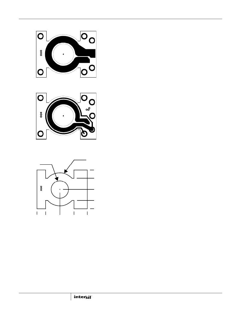
�FIGURE� 7E.� INT.� LAYER� 4:� 1� TURN� SECONDARY� WINDING�
�FIGURE� 7F.� BOTTOM� LAYER:� 1� TURN� SECONDARY� AND� SR�
�WINDINGS�
�?� 0.689�
�gate� charge� translates� into� higher� drive� requirements� and/or�
�slower� switching� speeds.� The� energy� required� to� drive� the� gates� is�
�dissipated� as� heat.�
�The� maximum� input� voltage,� V� IN� ,� plus� transient� voltage,�
�determines� the� voltage� rating� required.� With� a� maximum� input�
�voltage� of� 53V� for� this� application,� and� if� we� allow� a� 10%� adder�
�for� transients,� a� voltage� rating� of� 60V� or� higher� will� suffice.�
�The� RMS� current� through� the� each� primary� side� FET� can� be�
�determined� from� Equation� 17,� substituting� 5A� of� primary� current�
�for� I� OUT� .� The� result� is� 3.5A� RMS.� Fairchild� FDS3672� FETs,� rated� at�
�100V� and� 7.5A� (r� DS(ON)� =� 22m� Ω� ),� were� selected� for� the� half-�
�bridge� switches.�
�The� synchronous� rectifier� FETs� must� withstand� approximately�
�one� half� of� the� input� voltage� assuming� no� switching� transients�
�are� present.� This� suggests� a� device� capable� of� withstanding� at�
�least� 30V� is� required.� Empirical� testing� in� the� circuit� revealed�
�switching� transients� of� 20V� were� present� across� the� device�
�indicating� a� rating� of� at� least� 60V� is� required.�
�?� 0.358�
�0.807�
�0.639�
�0.403�
�The� RMS� current� rating� of� 7.07A� for� each� SR� FET� requires� a� low�
�r� DS(ON)� to� minimize� conduction� losses,� which� is� difficult� to� find� in� a�
�60V� device.� It� was� decided� to� use� two� devices� in� parallel� to� simplify�
�the� thermal� design.� Two� Fairchild� FDS5670� devices� are� used� in�
�parallel� for� a� total� of� four� SR� FETs.� The� FDS5670� is� rated� at� 60V�
�and� 10A� (r� DS(ON)� =� 14m� Ω� ).�
�Oscillator� Component� Selection�
�0.169�
�0.000�
�0.000� 0.184� 0.479� 0.774� 1.054�
�FIGURE� 7G.� PWB� DIMENSIONS�
�MOSFET� Selection�
�The� criteria� for� selection� of� the� primary� side� half-bridge� FETs� and�
�the� secondary� side� synchronous� rectifier� FETs� is� largely� based� on�
�the� current� and� voltage� rating� of� the� device.� However,� the� FET�
�drain-source� capacitance� and� gate� charge� cannot� be� ignored.�
�The� zero� voltage� switch� (ZVS)� transition� timing� is� dependent� on�
�the� transformer’s� leakage� inductance� and� the� capacitance� at� the�
�node� between� the� upper� FET� source� and� the� lower� FET� drain.� The�
�node� capacitance� is� comprised� of� the� drain-source� capacitance�
�of� the� FETs� and� the� transformer� parasitic� capacitance.� The�
�leakage� inductance� and� capacitance� form� an� LC� resonant� tank�
�circuit� which� determines� the� duration� of� the� transition.� The�
�amount� of� energy� stored� in� the� LC� tank� circuit� determines� the�
�17�
�The� desired� operating� frequency� of� 235kHz� for� the� converter� was�
�established� in� “Design� Criteria”� on� page� 14.� The� oscillator�
�frequency� operates� at� twice� the� frequency� of� the� converter�
�because� two� clock� cycles� are� required� for� a� complete� converter�
�period.�
�During� each� oscillator� cycle� the� timing� capacitor,� C� T� ,� must� be�
�charged� and� discharged.� Determining� the� required� discharge�
�time� to� achieve� zero� voltage� switching� (ZVS)� is� the� critical� design�
�goal� in� selecting� the� timing� components.� The� discharge� time� sets�
�the� deadtime� between� the� two� outputs,� and� is� the� same� as� ZVS�
�transition� time.� Once� the� discharge� time� is� determined,� the�
�remainder� of� the� period� becomes� the� charge� time.�
�The� ZVS� transition� duration� is� determined� by� the� transformer’s�
�primary� leakage� inductance,� L� lk� ,� by� the� FET� Coss,� by� the�
�transformer’s� parasitic� winding� capacitance,� and� by� any� other�
�parasitic� elements� on� the� node.� The� parameters� may� be�
�FN9111.6�
�December� 2,� 2011�
�相关PDF资料 |
PDF描述 |
|---|---|
| ISL6565BCVZ | IC REG CTRLR BUCK PWM VM 28TSSOP |
| ISL6565BCRZ | IC REG CTRLR BUCK PWM VM 28-QFN |
| ISL6565ACVZ | IC REG CTRLR BUCK PWM VM 28TSSOP |
| ISL6755AAZA-T | IC REG CTRLR PWM CM/VM 20-QSOP |
| ISL6306IRZ-T | IC REG CTRLR BUCK PWM VM 40-QFN |
相关代理商/技术参数 |
参数描述 |
|---|---|
| ISL6741IB-T | 功能描述:IC REG CTRLR PWM CM 16-SOIC RoHS:否 类别:集成电路 (IC) >> PMIC - 稳压器 - DC DC 切换控制器 系列:- 标准包装:2,500 系列:- PWM 型:电流模式 输出数:1 频率 - 最大:500kHz 占空比:100% 电源电压:8.2 V ~ 30 V 降压:无 升压:无 回扫:是 反相:无 倍增器:无 除法器:无 Cuk:无 隔离:是 工作温度:0°C ~ 70°C 封装/外壳:8-DIP(0.300",7.62mm) 包装:管件 产品目录页面:1316 (CN2011-ZH PDF) |
| ISL6741IBZ | 功能描述:IC REG CTRLR PWM CM 16-SOIC RoHS:是 类别:集成电路 (IC) >> PMIC - 稳压器 - DC DC 切换控制器 系列:- 产品培训模块:Lead (SnPb) Finish for COTS Obsolescence Mitigation Program 标准包装:2,500 系列:- PWM 型:电流模式 输出数:1 频率 - 最大:275kHz 占空比:50% 电源电压:18 V ~ 110 V 降压:无 升压:无 回扫:无 反相:无 倍增器:无 除法器:无 Cuk:无 隔离:是 工作温度:-40°C ~ 85°C 封装/外壳:8-SOIC(0.154",3.90mm 宽) 包装:带卷 (TR) |
| ISL6741IBZ-T | 功能描述:IC REG CTRLR PWM CM 16-SOIC RoHS:是 类别:集成电路 (IC) >> PMIC - 稳压器 - DC DC 切换控制器 系列:- 产品培训模块:Lead (SnPb) Finish for COTS Obsolescence Mitigation Program 标准包装:2,500 系列:- PWM 型:电流模式 输出数:1 频率 - 最大:275kHz 占空比:50% 电源电压:18 V ~ 110 V 降压:无 升压:无 回扫:无 反相:无 倍增器:无 除法器:无 Cuk:无 隔离:是 工作温度:-40°C ~ 85°C 封装/外壳:8-SOIC(0.154",3.90mm 宽) 包装:带卷 (TR) |
| ISL6741IV | 功能描述:IC REG CTRLR PWM CM 16-TSSOP RoHS:否 类别:集成电路 (IC) >> PMIC - 稳压器 - DC DC 切换控制器 系列:- 标准包装:2,500 系列:- PWM 型:电流模式 输出数:1 频率 - 最大:500kHz 占空比:100% 电源电压:8.2 V ~ 30 V 降压:无 升压:无 回扫:是 反相:无 倍增器:无 除法器:无 Cuk:无 隔离:是 工作温度:0°C ~ 70°C 封装/外壳:8-DIP(0.300",7.62mm) 包装:管件 产品目录页面:1316 (CN2011-ZH PDF) |
| ISL6741IV-T | 功能描述:IC REG CTRLR PWM CM 16-TSSOP RoHS:否 类别:集成电路 (IC) >> PMIC - 稳压器 - DC DC 切换控制器 系列:- 标准包装:2,500 系列:- PWM 型:电流模式 输出数:1 频率 - 最大:500kHz 占空比:100% 电源电压:8.2 V ~ 30 V 降压:无 升压:无 回扫:是 反相:无 倍增器:无 除法器:无 Cuk:无 隔离:是 工作温度:0°C ~ 70°C 封装/外壳:8-DIP(0.300",7.62mm) 包装:管件 产品目录页面:1316 (CN2011-ZH PDF) |
发布紧急采购,3分钟左右您将得到回复。