参数资料
| 型号: | ISL6741IV-T |
| 厂商: | Intersil |
| 文件页数: | 12/28页 |
| 文件大小: | 0K |
| 描述: | IC REG CTRLR PWM CM 16-TSSOP |
| 标准包装: | 2,500 |
| PWM 型: | 电流模式 |
| 输出数: | 2 |
| 频率 - 最大: | 2MHz |
| 占空比: | 100% |
| 电源电压: | 9 V ~ 16 V |
| 降压: | 无 |
| 升压: | 无 |
| 回扫: | 无 |
| 反相: | 无 |
| 倍增器: | 无 |
| 除法器: | 无 |
| Cuk: | 无 |
| 隔离: | 无 |
| 工作温度: | -40°C ~ 105°C |
| 封装/外壳: | 16-TSSOP(0.173",4.40mm 宽) |
| 包装: | 带卷 (TR) |
第1页第2页第3页第4页第5页第6页第7页第8页第9页第10页第11页当前第12页第13页第14页第15页第16页第17页第18页第19页第20页第21页第22页第23页第24页第25页第26页第27页第28页
�� �
�
�ISL6740,� ISL6741�
�where� t� C� and� t� D� are� the� charge� and� discharge� times,� respectively,�
�t� SW� is� the� oscillator� free� running� period,� and� f� is� the� oscillator�
�frequency.� One� output� switching� cycle� requires� two� oscillator�
�cycles.� The� actual� times� will� be� slightly� longer� than� calculated�
�due� to� internal� propagation� delays� of� approximately�
�10ns/transition.� This� delay� ads� directly� to� the� switching� duration,�
�but� also� causes� overshoot� of� the� timing� capacitor� peak� and� valley�
�voltage� thresholds,� effectively� increasing� the� peak-to-peak�
�voltage� on� the� timing� capacitor.� Additionally,� if� very� low� charge�
�and� discharge� currents� are� used,� there� will� be� increased� error�
�due� to� the� input� impedance� at� the� C� T� pin.�
�The� maximum� duty� cycle,� D,� and� percent� deadtime,� DT,� can� be�
�calculated� from:�
�recovery� from� a� Fault� condition� or� overcurrent/short� circuit�
�shutdown.� The� soft-start� voltage� is� clamped� to� 4.5V.�
�The� Fault� signal� output� is� high� impedance� during� the� soft-start�
�cycle.� A� pull-up� resistor� to� VREF� or� a� pull-down� resistor� to� ground�
�should� be� added� to� achieve� the� desired� state� of� Fault� during� soft-�
�start.�
�Gate� Drive�
�The� ISL6740,� ISL6741� are� capable� of� sourcing� and� sinking� 0.5A�
�peak� current,� but� are� primarily� intended� to� be� used� in�
�conjunction� with� a� MOSFET� driver� due� to� the� 5V� drive� level.� To�
�limit� the� peak� current� through� the� IC,� an� external� resistor� may� be�
�placed� between� the� totem-pole� output� of� the� IC� (OUTA� or� OUTB�
�t� C�
�t� SW�
�D� =� ----------�
�DT� =� 1� –� D�
�(EQ.� 5)�
�(EQ.� 6)�
�pin)� and� the� gate� of� the� MOSFET.� This� small� series� resistor� also�
�damps� any� oscillations� caused� by� the� resonant� tank� of� the�
�parasitic� inductances� in� the� traces� of� the� board� and� the� FET’s�
�input� capacitance.�
�Undervoltage� Monitor� and� Inhibit�
�Implementing� Synchronization�
�The� oscillator� can� be� synchronized� to� an� external� clock� applied� to�
�the� SYNC� pin� or� by� connecting� the� SYNC� pins� of� multiple� ICs�
�together.� If� an� external� master� clock� signal� is� used,� the� free�
�running� frequency� of� the� oscillator� should� be� ~10%� slower� than�
�the� desired� synchronous� frequency.� The� external� master� clock�
�signal� should� have� a� pulse� width� greater� than� 20ns.� The� SYNC�
�circuitry� will� not� respond� to� an� external� signal� during� the� first�
�60%� of� the� oscillator� switching� cycle.� Self-synchronization� is� not�
�recommended� for� oscillator� frequencies� above� 900� kHz.� For�
�higher� switching� frequencies,� an� external� clock� with� a� pulse�
�width� less� than� one-half� of� the� oscillator� period� must� be� used.�
�The� SYNC� input� is� edge� triggered� and� its� duration� does� not� affect�
�oscillator� operation.� However,� the� deadtime� is� affected� by� the�
�SYNC� frequency.� A� higher� frequency� signal� applied� to� the� SYNC�
�input� will� shorten� the� deadtime.� The� shortened� deadtime� is� the�
�result� of� the� timing� capacitor� charge� cycle� being� prematurely�
�terminated� by� the� external� SYNC� pulse.� Consequently,� the� timing�
�capacitor� is� not� fully� charged� when� the� discharge� cycle� begins.�
�This� effect� is� only� a� concern� when� an� external� master� clock� is�
�used,� or� if� units� with� different� operating� frequencies� are�
�paralleled.�
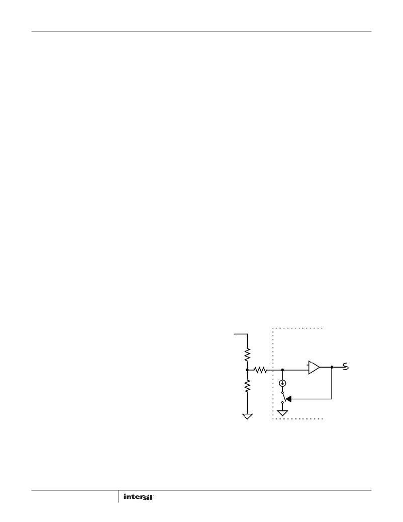
�The� UV� input� is� used� for� input� source� undervoltage� lockout� and�
�inhibit� functions.� If� the� node� voltage� falls� below� 1.00V� a� UV�
�shutdown� fault� occurs.� This� may� be� caused� by� low� source� voltage�
�or� by� intentional� grounding� of� the� pin� to� disable� the� outputs.�
�There� is� a� nominal� 10� μ� A� switched� current� source� used� to� create�
�hysteresis.� The� current� source� is� active� only� during� an� UV/Inhibit�
�fault;� otherwise,� it� is� inactive� and� does� not� affect� the� node�
�voltage.� The� magnitude� of� the� hysteresis� is� a� function� of� the�
�external� resistor� divider� impedance.� If� the� resistor� divider�
�impedance� results� in� too� little� hysteresis,� a� series� resistor�
�between� the� UV� pin� and� the� divider� may� be� used� to� increase� the�
�hysteresis.� A� soft-start� cycle� begins� when� the� UV/Inhibit� fault�
�clears.�
�The� voltage� hysteresis� created� by� the� switched� current� source�
�and� the� external� impedance� is� generally� small� due� to� the� large�
�resistor� divider� ratio� required� to� scale� the� input� voltage� down� to�
�the� UV� threshold� level.� A� small� capacitor� placed� between� the� UV�
�input� and� ground� may� be� required� to� filter� noise� out.�
�V� IN�
�R1�
�Soft-start� Operation�
�The� ISL6740,� ISL6741� feature� a� soft-start� using� an� external�
�R3�
�1.00V�
�+�
�-�
�capacitor� in� conjunction� with� an� internal� current� source.� soft-start�
�reduces� stresses� and� surge� currents� during� start� up.�
�Upon� start� up,� the� soft-start� circuitry� clamps� the� error� voltage�
�input� (V� ERROR� pin)� indirectly� to� a� value� equal� to� the� soft-start�
�voltage.� The� soft-start� clamp� does� not� actually� clamp� the� error�
�R2�
�10� μ� A�
�ON�
�voltage� input� as� is� done� in� many� implementations.� Rather� the�
�PWM� comparator� has� two� inverting� inputs� such� that� the� lower�
�voltage� is� in� control.�
�FIGURE� 5.� UV� HYSTERESIS�
�As� V� IN� decreases� to� a� UV� condition,� the� threshold� level� is:�
�V� IN� (� DOWN� )� =� ----------------------�
�The� output� pulse� width� increases� as� the� soft-start� capacitor�
�voltage� increases.� This� has� the� effect� of� increasing� the� duty� cycle�
�from� zero� to� the� regulation� pulse� width� during� the� soft-start�
�R1� +� R2�
�R2�
�V�
�(EQ.� 7)�
�period.� When� the� soft-start� voltage� exceeds� the� error� voltage,�
�soft-start� is� completed.� soft-start� occurs� during� start-up,� after�
�12�
�FN9111.6�
�December� 2,� 2011�
�相关PDF资料 |
PDF描述 |
|---|---|
| ISL6742AAZA-T | IC REG CTRLR PWM CM/VM 16-QSOP |
| ISL6744AABZ | IC REG CTRLR PWM VM 8-SOIC |
| ISL6744AU-T | IC REG CTRLR BUCK PWM VM 8-MSOP |
| ISL6745AAUZ | IC REG CTRLR PWM VM 10-MSOP |
| ISL6745AU-T | IC REG CTRLR PWM VM 10-MSOP |
相关代理商/技术参数 |
参数描述 |
|---|---|
| ISL6741IVZ | 功能描述:IC REG CTRLR PWM CM 16-TSSOP RoHS:是 类别:集成电路 (IC) >> PMIC - 稳压器 - DC DC 切换控制器 系列:- 产品培训模块:Lead (SnPb) Finish for COTS Obsolescence Mitigation Program 标准包装:2,500 系列:- PWM 型:电流模式 输出数:1 频率 - 最大:275kHz 占空比:50% 电源电压:18 V ~ 110 V 降压:无 升压:无 回扫:无 反相:无 倍增器:无 除法器:无 Cuk:无 隔离:是 工作温度:-40°C ~ 85°C 封装/外壳:8-SOIC(0.154",3.90mm 宽) 包装:带卷 (TR) |
| ISL6741IVZ-T | 功能描述:IC REG CTRLR PWM CM 16-TSSOP RoHS:是 类别:集成电路 (IC) >> PMIC - 稳压器 - DC DC 切换控制器 系列:- 产品培训模块:Lead (SnPb) Finish for COTS Obsolescence Mitigation Program 标准包装:2,500 系列:- PWM 型:电流模式 输出数:1 频率 - 最大:275kHz 占空比:50% 电源电压:18 V ~ 110 V 降压:无 升压:无 回扫:无 反相:无 倍增器:无 除法器:无 Cuk:无 隔离:是 工作温度:-40°C ~ 85°C 封装/外壳:8-SOIC(0.154",3.90mm 宽) 包装:带卷 (TR) |
| ISL6742AAZA | 功能描述:IC REG CTRLR PWM CM/VM 16-QSOP RoHS:是 类别:集成电路 (IC) >> PMIC - 稳压器 - DC DC 切换控制器 系列:- 标准包装:75 系列:- PWM 型:电流模式 输出数:1 频率 - 最大:1MHz 占空比:81% 电源电压:4.3 V ~ 13.5 V 降压:是 升压:是 回扫:是 反相:无 倍增器:无 除法器:无 Cuk:无 隔离:无 工作温度:0°C ~ 70°C 封装/外壳:8-SOIC(0.154",3.90mm 宽) 包装:管件 产品目录页面:1051 (CN2011-ZH PDF) 其它名称:296-2543-5 |
| ISL6742AAZA-T | 功能描述:IC REG CTRLR PWM CM/VM 16-QSOP RoHS:是 类别:集成电路 (IC) >> PMIC - 稳压器 - DC DC 切换控制器 系列:- 产品培训模块:Lead (SnPb) Finish for COTS Obsolescence Mitigation Program 标准包装:2,500 系列:- PWM 型:电流模式 输出数:1 频率 - 最大:275kHz 占空比:50% 电源电压:18 V ~ 110 V 降压:无 升压:无 回扫:无 反相:无 倍增器:无 除法器:无 Cuk:无 隔离:是 工作温度:-40°C ~ 85°C 封装/外壳:8-SOIC(0.154",3.90mm 宽) 包装:带卷 (TR) |
| ISL6744AABZ | 功能描述:IC REG CTRLR PWM VM 8-SOIC RoHS:是 类别:集成电路 (IC) >> PMIC - 稳压器 - DC DC 切换控制器 系列:- 产品培训模块:Lead (SnPb) Finish for COTS Obsolescence Mitigation Program 标准包装:2,500 系列:- PWM 型:电流模式 输出数:1 频率 - 最大:275kHz 占空比:50% 电源电压:18 V ~ 110 V 降压:无 升压:无 回扫:无 反相:无 倍增器:无 除法器:无 Cuk:无 隔离:是 工作温度:-40°C ~ 85°C 封装/外壳:8-SOIC(0.154",3.90mm 宽) 包装:带卷 (TR) |
发布紧急采购,3分钟左右您将得到回复。