- 您现在的位置:买卖IC网 > PDF目录15735 > ISL6752EVAL1Z (Intersil)EVALUATION BOARD FOR ISL6752 PDF资料下载
参数资料
| 型号: | ISL6752EVAL1Z |
| 厂商: | Intersil |
| 文件页数: | 12/16页 |
| 文件大小: | 0K |
| 描述: | EVALUATION BOARD FOR ISL6752 |
| 标准包装: | 1 |
| 主要目的: | DC/DC,步降 |
| 输出及类型: | 1,非隔离 |
| 功率 - 输出: | 720W |
| 输出电压: | 12V |
| 电流 - 输出: | 60A |
| 输入电压: | 325 ~ 425V |
| 稳压器拓扑结构: | 降压 |
| 板类型: | 完全填充 |
| 已供物品: | 板 |
| 已用 IC / 零件: | ISL6752 |
�� �
�
�ISL6752�
�Determine� the� amount� of� voltage,� V� e� ,� that� must� be� added� to�
�and� Equation� 21� becomes:�
�(� 2D� –� V� e� +� Δ� V� CS� )� ?� R6�
�V� e� –� Δ� V� CS�
�the� current� feedback� signal� using� Equation� 13.�
�V� e� =� 153mV�
�R9� =� -------------------------------------------------------------�
�Ω�
�(EQ.� 24)�
�Next,� determine� the� effect� of� the� magnetizing� current� from�
�Equation� 18.�
�Δ� V� CS� =� 91mV�
�Using� Equation� 21,� solve� for� the� summing� resistor,� R9,� from�
�CTBUF� to� CS.�
�R9� =� 30.1k� Ω�
�Determine� the� new� value� of� R� CS� ,� R’� CS� ,� using� Equation� 22.�
�R’� CS� =� 15.4� Ω�
�This� discussion� determines� the� minimum� external� ramp� that�
�is� required.� Additional� slope� compensation� may� be�
�considered� for� design� margin.�
�If� the� application� requires� deadtime� of� less� than� about�
�500ns,� the� CTBUF� signal� may� not� perform� adequately� for�
�slope� compensation.� CTBUF� lags� the� CT� sawtooth�
�waveform� by� 300ns� to� 400ns.� This� behavior� results� in� a�
�non-zero� value� of� CTBUF� when� the� next� half-cycle� begins�
�The� buffer� transistor� used� to� create� the� external� ramp� from�
�CT� should� have� a� sufficiently� high� gain� (>200)� so� as� to�
�minimize� the� required� base� current.� Whatever� base� current�
�is� required� reduces� the� charging� current� into� CT� and� will�
�reduce� the� oscillator� frequency.�
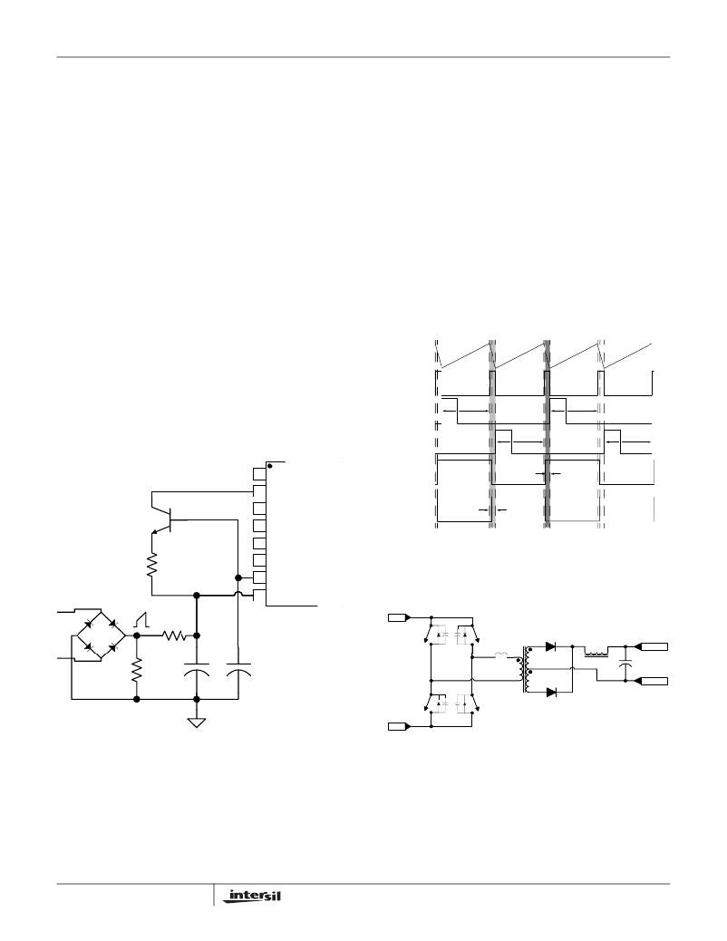
�ZVS� Full-Bridge� Operation�
�The� ISL6752� is� a� full-bridge� zero-voltage� switching� (ZVS)�
�PWM� controller� that� behaves� much� like� a� traditional� hard�
�switched� topology� controller.� Rather� than� drive� the� diagonal�
�bridge� switches� simultaneously,� the� upper� switches� (OUTUL,�
�OUTUR)� are� driven� at� a� fixed� 50%� duty� cycle� and� the� lower�
�switches� (OUTLL,� OUTLR)� are� pulse� width� modulated� on�
�the� trailing� edge.�
�CT�
�DEADTIME�
�when� the� deadtime� is� short.�
�Under� these� situations,� slope� compensation� may� be� added�
�by� externally� buffering� the� CT� signal� as� shown� in� Figure� 7.�
�1�
�2� VREF�
�OUTLL�
�OUTLR�
�OUTUR�
�PWM�
�PWM�
�PWM�
�RESONANT�
�DELAY�
�PWM�
�3�
�ISL6752�
�OUTUL�
�RESDEL�
�4�
�5�
�WINDOW�
�FIGURE� 8.� BRIDGE� DRIVE� SIGNAL� TIMING�
�R9�
�6�
�7� CT�
�To� understand� how� the� ZVS� method� operates,� one� must�
�R6�
�8� CS�
�include� the� parasitic� elements� of� the� circuit� and� examine� a�
�full� switching� cycle.�
�VIN+�
�UL�
�UR�
�L� L�
�D1�
�VOUT+�
�R� CS�
�C4�
�CT�
�VIN-�
�LL�
�LR�
�D2�
�RTN�
�FIGURE� 7.� ADDING� SLOPE� COMPENSATION� USING� CT�
�Using� CT� to� provide� slope� compensation� instead� of� CTBUF�
�requires� the� same� calculations,� except� that� Equations� 20�
�and� 21� require� modification.� Equation� 20� becomes:�
�FIGURE� 9.� IDEALIZED� FULL-BRIDGE�
�In� Figure� 9,� the� power� semiconductor� switches� have� been�
�replaced� by� ideal� switch� elements� with� parallel� diodes� and�
�capacitance,� the� output� rectifiers� are� ideal,� and� the�
�V� e� –� Δ� V� CS� =� ----------------------�
�2D� ?� R6�
�R6� +� R9�
�V�
�(EQ.� 23)�
�transformer� leakage� inductance� has� been� included� as� a�
�discrete� element.� The� parasitic� capacitance� has� been�
�lumped� together� as� switch� capacitance,� but� represents� all�
�parasitic� capacitance� in� the� circuit� including� winding�
�12�
�FN9181.3�
�October� 31,� 2008�
�相关PDF资料 |
PDF描述 |
|---|---|
| 1838283-1 | CONN FEMALE M8 3POS STR 2M CABLE |
| ISC1812ERR10K | INDUCTOR WW 100NH 10% 1812 |
| V375C15E75BL3 | CONVERTER MOD DC/DC 15V 75W |
| VI-BTM-EW-S | CONVERTER MOD DC/DC 10V 100W |
| GBM28DRYN | CONN EDGECARD 56POS DIP .156 SLD |
相关代理商/技术参数 |
参数描述 |
|---|---|
| ISL6753AAZA | 功能描述:IC REG CTRLR PWM CM/VM 16-QSOP RoHS:是 类别:集成电路 (IC) >> PMIC - 稳压器 - DC DC 切换控制器 系列:- 产品培训模块:Lead (SnPb) Finish for COTS Obsolescence Mitigation Program 标准包装:2,500 系列:- PWM 型:电流模式 输出数:1 频率 - 最大:275kHz 占空比:50% 电源电压:18 V ~ 110 V 降压:无 升压:无 回扫:无 反相:无 倍增器:无 除法器:无 Cuk:无 隔离:是 工作温度:-40°C ~ 85°C 封装/外壳:8-SOIC(0.154",3.90mm 宽) 包装:带卷 (TR) |
| ISL6753AAZA-T | 功能描述:IC REG CTRLR PWM CM/VM 16-QSOP RoHS:是 类别:集成电路 (IC) >> PMIC - 稳压器 - DC DC 切换控制器 系列:- 产品培训模块:Lead (SnPb) Finish for COTS Obsolescence Mitigation Program 标准包装:2,500 系列:- PWM 型:电流模式 输出数:1 频率 - 最大:275kHz 占空比:50% 电源电压:18 V ~ 110 V 降压:无 升压:无 回扫:无 反相:无 倍增器:无 除法器:无 Cuk:无 隔离:是 工作温度:-40°C ~ 85°C 封装/外壳:8-SOIC(0.154",3.90mm 宽) 包装:带卷 (TR) |
| ISL6754AAZA | 功能描述:IC REG CTRLR PWM CM/VM 20-QSOP RoHS:是 类别:集成电路 (IC) >> PMIC - 稳压器 - DC DC 切换控制器 系列:- 产品培训模块:Lead (SnPb) Finish for COTS Obsolescence Mitigation Program 标准包装:2,500 系列:- PWM 型:电流模式 输出数:1 频率 - 最大:275kHz 占空比:50% 电源电压:18 V ~ 110 V 降压:无 升压:无 回扫:无 反相:无 倍增器:无 除法器:无 Cuk:无 隔离:是 工作温度:-40°C ~ 85°C 封装/外壳:8-SOIC(0.154",3.90mm 宽) 包装:带卷 (TR) |
| ISL6754AAZA-T | 功能描述:IC REG CTRLR PWM CM/VM 20-QSOP RoHS:是 类别:集成电路 (IC) >> PMIC - 稳压器 - DC DC 切换控制器 系列:- 产品培训模块:Lead (SnPb) Finish for COTS Obsolescence Mitigation Program 标准包装:2,500 系列:- PWM 型:电流模式 输出数:1 频率 - 最大:275kHz 占空比:50% 电源电压:18 V ~ 110 V 降压:无 升压:无 回扫:无 反相:无 倍增器:无 除法器:无 Cuk:无 隔离:是 工作温度:-40°C ~ 85°C 封装/外壳:8-SOIC(0.154",3.90mm 宽) 包装:带卷 (TR) |
| ISL6754DBEVAL1Z | 功能描述:BOARD DEMO FOR ISL6754 RoHS:是 类别:编程器,开发系统 >> 评估板 - DC/DC 与 AC/DC(离线)SMPS 系列:* 标准包装:1 系列:- 主要目的:DC/DC,步降 输出及类型:1,非隔离 功率 - 输出:- 输出电压:3.3V 电流 - 输出:3A 输入电压:4.5 V ~ 28 V 稳压器拓扑结构:降压 频率 - 开关:250kHz 板类型:完全填充 已供物品:板 已用 IC / 零件:L7981 其它名称:497-12113STEVAL-ISA094V1-ND |
发布紧急采购,3分钟左右您将得到回复。