- 您现在的位置:买卖IC网 > PDF目录15203 > ISL6842IBZ (Intersil)IC REG CTRLR BST FLYBK ISO 8SOIC PDF资料下载
参数资料
| 型号: | ISL6842IBZ |
| 厂商: | Intersil |
| 文件页数: | 9/13页 |
| 文件大小: | 0K |
| 描述: | IC REG CTRLR BST FLYBK ISO 8SOIC |
| 标准包装: | 980 |
| PWM 型: | 电流模式 |
| 输出数: | 1 |
| 频率 - 最大: | 2MHz |
| 占空比: | 100% |
| 电源电压: | 15 V ~ 18 V |
| 降压: | 是 |
| 升压: | 是 |
| 回扫: | 是 |
| 反相: | 无 |
| 倍增器: | 无 |
| 除法器: | 无 |
| Cuk: | 无 |
| 隔离: | 是 |
| 工作温度: | -40°C ~ 105°C |
| 封装/外壳: | 8-SOIC(0.154",3.90mm 宽) |
| 包装: | 管件 |
�� �
�
�ISL6840,� ISL6841,� ISL6842,� ISL6843,� ISL6844,� ISL6845�
�Pin� Descriptions�
�RTCT� -� This� is� the� oscillator� timing� control� pin.� The�
�operational� frequency� and� maximum� duty� cycle� are� set� by�
�connecting� a� resistor,� RT,� between� VREF� and� this� pin� and� a�
�timing� capacitor,� CT,� from� this� pin� to� GND.� The� oscillator�
�produces� a� sawtooth� waveform� with� a� programmable�
�frequency� range� up� to� 2.0MHz.� The� charge� time,� t� C� ,� the�
�discharge� time,� t� D� ,� the� switching� frequency,� f,� and� the�
�maximum� duty� cycle,� Dmax,� can� be� calculated� from�
�Equations� 1,� 2,� 3� and� 4:�
�Functional� Description�
�Features�
�The� ISL684x� current� mode� PWMs� make� an� ideal� choice� for�
�low-cost� flyback� and� forward� topology� applications.� With� its�
�greatly� improved� performance� over� industry� standard� parts,�
�it� is� the� obvious� choice� for� new� designs� or� existing� designs�
�which� require� updating.�
�Oscillator�
�The� ISL684x� family� of� controllers� have� a� sawtooth� oscillator�
�t�
�C�
�≈� 0.583� ?� RT� ?� CT�
�(EQ.� 1)�
�with� a� programmable� frequency� range� to� 2MHz,� which� can�
�be� programmed� with� a� resistor� from� VREF� and� a� capacitor� to�
�t� D� ≈� –� RT� ?� CT� ?� ln� ?� ----------------------------------------------� ?�
�D� =� t� ?� f�
�f� =� 1� ?� (� tC� +� tD� )�
�C�
�0.0083� ?� RT� –� 4.3�
�?� 0.0083� ?� RT� –� 2.4� ?�
�(EQ.� 2)�
�(EQ.� 3)�
�(EQ.� 4)�
�GND� on� the� RTCT� pin.� (Please� refer� to� Figure� 4� for� the�
�resistor� and� capacitance� required� for� a� given� frequency.)�
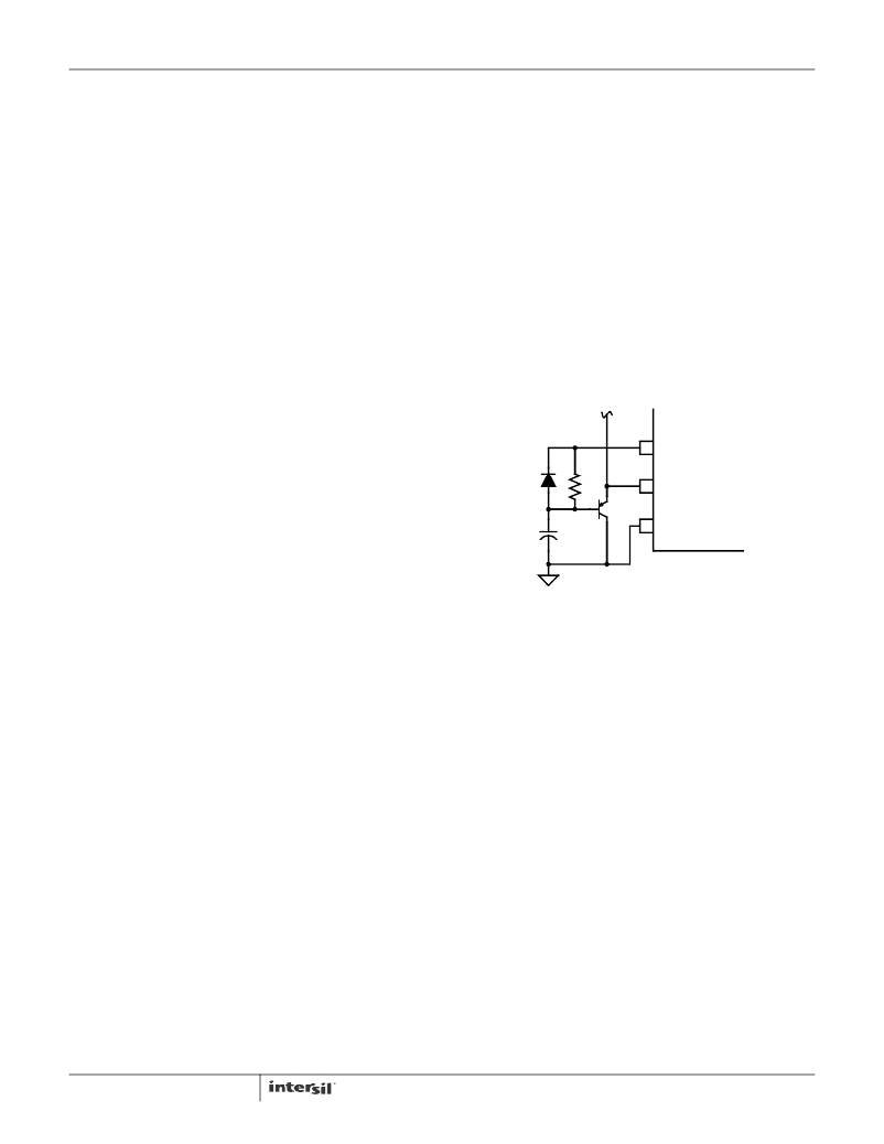
�Soft-Start� Operation�
�Soft-start� must� be� implemented� externally.� One� method,�
�illustrated� in� Figure� 5,� clamps� the� voltage� on� COMP.�
�Figure� 4� may� be� used� as� a� guideline� in� selecting� the�
�capacitor� and� resistor� values� required� for� a� given� frequency.�
�COMP� -� COMP� is� the� output� of� the� error� amplifier� and� the�
�input� of� the� PWM� comparator.� The� control� loop� frequency�
�compensation� network� is� connected� between� the� COMP� and�
�FB� pins.�
�FB� -� The� output� voltage� feedback� is� connected� to� the�
�VREF�
�COMP�
�GND�
�inverting� input� of� the� error� amplifier� through� this� pin.� The�
�non-inverting� input� of� the� error� amplifier� is� internally� tied� to� a�
�reference� voltage.�
�FIGURE� 5.� SOFT-START�
�CS� -� This� is� the� current� sense� input� to� the� PWM� comparator.�
�The� range� of� the� input� signal� is� nominally� 0V� to� 1.0V� and� has�
�an� internal� offset� of� 100mV.�
�GND� -� GND� is� the� power� and� small� signal� reference� ground�
�for� all� functions.�
�OUT� -� This� is� the� drive� output� to� the� power� switching� device.�
�It� is� a� high� current� output� capable� of� driving� the� gate� of� a�
�power� MOSFET� with� peak� currents� of� 1.0A.�
�VDD� -� V� DD� is� the� power� connection� for� the� device.� The� total�
�supply� current� will� depend� on� the� load� applied� to� OUT.� Total�
�I� DD� current� is� the� sum� of� the� operating� current� and� the�
�average� output� current.� Knowing� the� operating� frequency,� f,�
�and� the� MOSFET� gate� charge,� Qg,� the� average� output�
�current� can� be� calculated� in� Equation� 5:�
�I� OUT� =� Qg� � f� (EQ.� 5)�
�To� optimize� noise� immunity,� bypass� V� DD� to� GND� with� a�
�ceramic� capacitor� as� close� to� the� VDD� and� GND� pins� as�
�possible.�
�VREF� -� The� 5.00V� reference� voltage� output.� +1.0/-1.5%�
�tolerance� over� line,� load� and� operating� temperature.� Bypass�
�to� GND� with� a� 0.1μF� to� 3.3μF� capacitor� to� filter� this� output� as�
�needed.�
�9�
�Gate� Drive�
�The� ISL684x� family� are� capable� of� sourcing� and� sinking� 1A�
�peak� current.� To� limit� the� peak� current� through� the� IC,� an�
�optional� external� resistor� may� be� placed� between� the�
�totem-pole� output� of� the� IC� (OUT� pin)� and� the� gate� of� the�
�MOSFET.� This� small� series� resistor� also� damps� any�
�oscillations� caused� by� the� resonant� tank� of� the� parasitic�
�inductances� in� the� traces� of� the� board� and� the� FET’s� input�
�capacitance.�
�Slope� Compensation�
�For� applications� where� the� maximum� duty� cycle� is� less� than�
�50%,� slope� compensation� may� be� used� to� improve� noise�
�immunity,� particularly� at� lighter� loads.� The� amount� of� slope�
�compensation� required� for� noise� immunity� is� determined�
�empirically,� but� is� generally� about� 10%� of� the� full� scale�
�current� feedback� signal.� For� applications� where� the� duty�
�cycle� is� greater� than� 50%,� slope� compensation� is� required� to�
�prevent� instability.� The� minimum� amount� of� slope�
�compensation� required� corresponds� to� 1/2� the� inductor�
�downslope.� Adding� excessive� slope� compensation,�
�however,� results� in� a� control� loop� that� behaves� more� as� a�
�voltage� mode� controller� than� as� a� current� mode� controller.�
�Slope� compensation� may� be� added� to� the� CS� signal� shown�
�in� Figure� 7.�
�FN9124.11�
�February� 23,� 2012�
�相关PDF资料 |
PDF描述 |
|---|---|
| CAT1232LPW-T2 | IC SUPERVISOR MPU 5V 16SOIC |
| GMC18DRTI | CONN EDGECARD 36POS DIP .100 SLD |
| CAT1232LPV-GT3 | IC SUPERVISOR 5V 8-SOIC |
| ISL6841IUZ | IC REG CTRLR BST FLYBK ISO 8MSOP |
| GCC30DRTI | CONN EDGECARD 60POS DIP .100 SLD |
相关代理商/技术参数 |
参数描述 |
|---|---|
| ISL6842IBZ-T | 功能描述:IC REG CTRLR BST FLYBK ISO 8SOIC RoHS:是 类别:集成电路 (IC) >> PMIC - 稳压器 - DC DC 切换控制器 系列:- 产品培训模块:Lead (SnPb) Finish for COTS Obsolescence Mitigation Program 标准包装:2,500 系列:- PWM 型:电流模式 输出数:1 频率 - 最大:275kHz 占空比:50% 电源电压:18 V ~ 110 V 降压:无 升压:无 回扫:无 反相:无 倍增器:无 除法器:无 Cuk:无 隔离:是 工作温度:-40°C ~ 85°C 封装/外壳:8-SOIC(0.154",3.90mm 宽) 包装:带卷 (TR) |
| ISL6842IRZ | 制造商:Rochester Electronics LLC 功能描述:- Bulk 制造商:Intersil Corporation 功能描述: |
| ISL6842IRZ-T | 功能描述:IC REG CTRLR BST FLYBK ISO 8-DFN RoHS:是 类别:集成电路 (IC) >> PMIC - 稳压器 - DC DC 切换控制器 系列:- 产品培训模块:Lead (SnPb) Finish for COTS Obsolescence Mitigation Program 标准包装:2,500 系列:- PWM 型:电流模式 输出数:1 频率 - 最大:275kHz 占空比:50% 电源电压:18 V ~ 110 V 降压:无 升压:无 回扫:无 反相:无 倍增器:无 除法器:无 Cuk:无 隔离:是 工作温度:-40°C ~ 85°C 封装/外壳:8-SOIC(0.154",3.90mm 宽) 包装:带卷 (TR) |
| ISL6842IU | 功能描述:IC REG CTRLR BST FLYBK ISO 8MSOP RoHS:否 类别:集成电路 (IC) >> PMIC - 稳压器 - DC DC 切换控制器 系列:- 标准包装:2,500 系列:- PWM 型:电流模式 输出数:1 频率 - 最大:500kHz 占空比:100% 电源电压:8.2 V ~ 30 V 降压:无 升压:无 回扫:是 反相:无 倍增器:无 除法器:无 Cuk:无 隔离:是 工作温度:0°C ~ 70°C 封装/外壳:8-DIP(0.300",7.62mm) 包装:管件 产品目录页面:1316 (CN2011-ZH PDF) |
| ISL6842IU-T | 功能描述:IC REG CTRLR BST FLYBK ISO 8MSOP RoHS:否 类别:集成电路 (IC) >> PMIC - 稳压器 - DC DC 切换控制器 系列:- 标准包装:2,500 系列:- PWM 型:电流模式 输出数:1 频率 - 最大:500kHz 占空比:100% 电源电压:8.2 V ~ 30 V 降压:无 升压:无 回扫:是 反相:无 倍增器:无 除法器:无 Cuk:无 隔离:是 工作温度:0°C ~ 70°C 封装/外壳:8-DIP(0.300",7.62mm) 包装:管件 产品目录页面:1316 (CN2011-ZH PDF) |
发布紧急采购,3分钟左右您将得到回复。