- 您现在的位置:买卖IC网 > PDF目录13603 > ISL8016IR18Z-T (Intersil)IC REG BUCK SYNC 1.8V 6A 20QFN PDF资料下载
参数资料
| 型号: | ISL8016IR18Z-T |
| 厂商: | Intersil |
| 文件页数: | 19/22页 |
| 文件大小: | 0K |
| 描述: | IC REG BUCK SYNC 1.8V 6A 20QFN |
| 产品培训模块: | Solutions for Industrial Control Applications |
| 标准包装: | 6,000 |
| 类型: | 降压(降压) |
| 输出类型: | 固定 |
| 输出数: | 1 |
| 输出电压: | 1.8V |
| 输入电压: | 2.7 V ~ 5.5 V |
| PWM 型: | 电流模式 |
| 频率 - 开关: | 525kHz ~ 3.9MHz |
| 电流 - 输出: | 6A |
| 同步整流器: | 是 |
| 工作温度: | -40°C ~ 85°C |
| 安装类型: | 表面贴装 |
| 封装/外壳: | 20-VFQFN 裸露焊盘 |
| 包装: | 带卷 (TR) |
| 供应商设备封装: | 20-QFN(3x4) |
�� �
�
�ISL8016�
�d� 1�
�F� m� =� ?� ----------------� =� ------------------------------�
�(� S� e� +� S� n� )� T� s�
�1� +� ------------�
�L� v� (� S� )� =� ---------� -----------------------� ----------------------� ---------------� ,� ω� p� ≈� -------------�
�V� FB� R� o� +� R� LP� ω� esr� A� v� (� S� )� 1�
�S� H� e� (� S� )�
�PWM� COMPARATOR� GAIN� F� m� :�
�The� PWM� comparator� gain� F� m� for� peak� current� mode� control� is�
�given� by� Equation� 6:�
�(EQ.� 6)�
�v� comp�
�Where,� S� e� is� the� slew� rate� of� the� slope� compensation� and� S� n� is�
�given� by� Equation� 7:�
�S�
�(EQ.� 14)�
�V� o� R� t� 1� +� -------� R� o� C� o�
�ω� p�
�From� Equation� 14,� it� is� shown� that� the� system� is� a� single� order�
�system,� which� has� a� single� pole� located� at� ω� p� before� the� half�
�switching� frequency.� Therefore,� a� simple� type� II� compensator� can�
�be� easily� used� to� stabilize� the� system.�
�L�
�V� in� –� V� o�
�S� n� =� R� t� --------------------�
�P�
�(EQ.� 7)�
�Vo�
�Where� R� t� is� trans-resistance,� which� is� the� gain� of� the� current�
�amplifier.�
�R� 2�
�C� 3�
�S�
�S�
�ω� n� Q� n�
�where� Q� n� and� ω� n� are� given� by� Q� n� =� –� ---� ,� ω� n� =� π� f� s�
�CURRENT� SAMPLING� TRANSFER� FUNCTION� H� e� (S):�
�In� current� loop,� the� current� signal� is� sampled� every� switching�
�cycle.� It� has� the� following� transfer� function:�
�2�
�2�
�H� e� (� S� )� =� -------� +� --------------� +� 1�
�(EQ.� 8)�
�ω� n�
�2�
�π�
�R� 3�
�V� FB�
�VREF�
�-�
�+�
�GM�
�VCOMP�
�R� 6�
�C� 6�
�C� 7�
�Power� Stage� Transfer� Functions�
�1� +� ------------�
�v� o� ω� esr�
�F� 1� (� S� )� =� ------� =� V� in� --------------------------------------�
�d� ?�
�S�
�S�
�ω� o� Q� p�
�-------� +� --------------� +� 1�
�ω� o�
�1�
�1�
�Where� ω� esr� =� -------------� ,� Q� p� ≈� R� o� -----� o� -� ,� ω� o� =� -----------------�
�1� +� ------�
�F� 2� (� S� )� =� ---� ?� -� =� -----------------------� --------------------------------------�
�?� o� V� in� ω� z�
�R� o� +� R� LP�
�d�
�S�
�S�
�ω� o� Q� p�
�-------� +� --------------� +� 1�
�ω� o�
�?� 1� +� ------------� ?� ?� 1� +� ------------� ?�
�ω� cz1� ?� ?�
�ω� cz2� ?�
�v� ?� comp�
�?�
�A� v� (� S� )� =� ----------------� =� -------------------� ---------------------------------------------------------�
�C� 6� +� C� 7�
�v� ?� FB�
�S� ?� 1� +� ----------� ?�
�ω� cp�
�C� +� C�
�Where� ω� cz1� =� --------------� ,� ω� cz2� =� --------------� ,� ω� cp� =� ---------------------� 7�
�Loop� bandwidth� f� c� :� ?� ?� 4� ---� to� -------� ?� ?� f� s�
�Transfer� function� F� 1� (S)� from� control� to� output� voltage� is:�
�S�
�(EQ.� 9)�
�2�
�2�
�C�
�R� c� C� o� L� P� L� P� C� o�
�Transfer� function� F� 2� (S)� from� control� to� inductor� current� is� given�
�by� Equation� 10:�
�S�
�(EQ.� 10)�
�2�
�2�
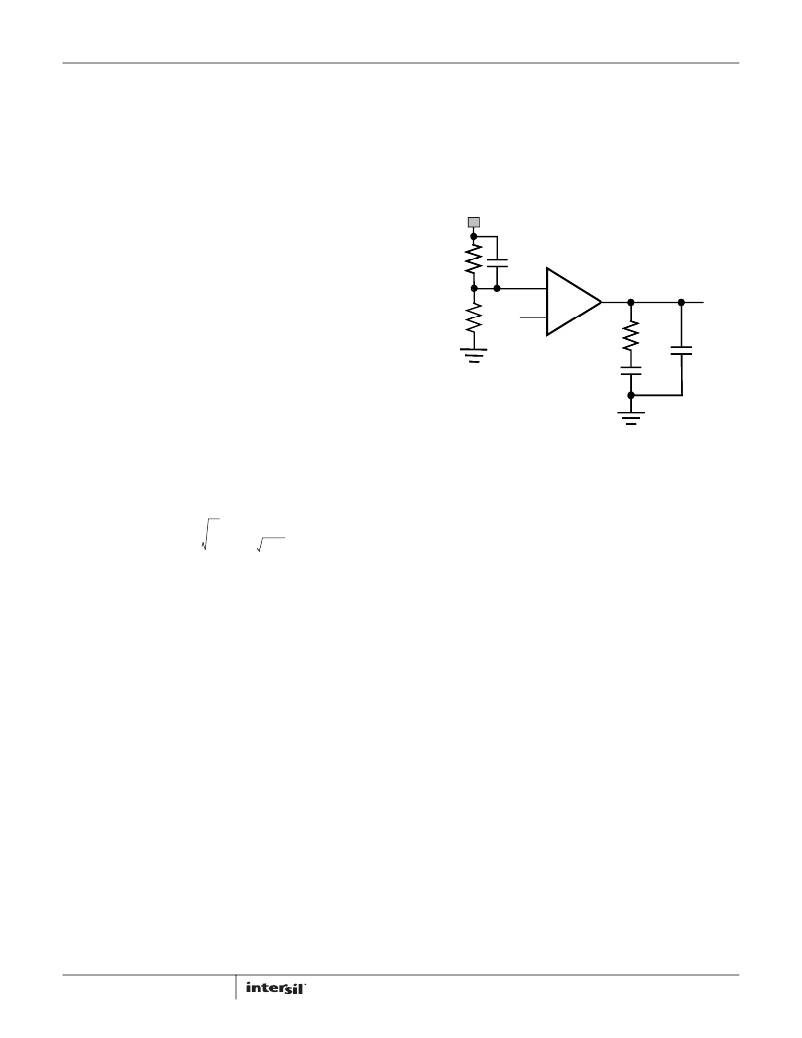
�FIGURE� 41.� TYPE� II� COMPENSATOR�
�Figure� 41� shows� the� type� II� compensator� and� its� transfer� function�
�is� expressed� as� follows:�
�S� S�
�GM� (EQ.� 15)�
�S�
�?� ?�
�1� 1� 6�
�R� 6� C� 6� R� 2� C� 3� R� 6� C� 6� C� 7�
�Compensator� design� goal:�
�High� DC� gain�
�1� 1�
�10�
�where� ω� z� =� -------------� .�
�Put� compensator� zero� ω� cz1� =� (� 1to3� )� -------------�
�R� C�
�1�
�R� o� C� o�
�Current� loop� gain� T� i� (S)� is� expressed� as� Equation� 11:�
�T� i� (� S� )� =� R� t� F� m� F� 2� (� S� )� H� e� (� S� )�
�The� voltage� loop� gain� with� open� current� loop� is:�
�T� v� (� S� )� =� KF� m� F� 1� (� S� )� A� v� (� S� )�
�(EQ.� 11)�
�(EQ.� 12)�
�Gain� margin:� >10dB�
�Phase� margin:� 40°�
�The� compensator� design� procedure� is� as� follows:�
�1�
�o� o�
�Put� one� compensator� pole� at� zero� frequency� to� achieve� high� DC�
�gain,� and� put� another� compensator� pole� at� either� ESR� zero�
�L� v� (� S� )� =� -----------------------�
�T� v� (� S� )�
�1� +� T� i� (� S� )�
�K� =� ---------� ,� V� FB�
�V� o�
�Put� compensator� zero� ω� cz2� =� (� 5to8� )� -------------�
�R� C�
�2� π� f� c� V� o� C� o� R� t�
�R� 6� =� --------------------------------�
�GM� ?� V� FB�
�The� Voltage� loop� gain� with� current� loop� closed� is� given� by�
�Equation� 13:�
�(EQ.� 13)�
�V� FB�
�Where� is� the� feedback� voltage� of� the� voltage�
�error� amplifier.� If� T� i� (S)>>1,� then� Equation� 13� can� be� simplified� by�
�Equation� 14:�
�19�
�frequency� or� half� switching� frequency,� whichever� is� lower.� An�
�optional� zero� can� boost� the� phase� margin.� ω� CZ2� is� a� zero� due� to�
�R� 2� and� C� 3� .�
�1�
�o� o�
�The� loop� gain� T� v� (S)� at� cross� over� frequency� of� f� c� has� unity� gain.�
�Therefore,� the� compensator� resistance� R� 6� is� determined� by:�
�(EQ.� 16)�
�FN7616.1�
�May� 5,� 2011�
�相关PDF资料 |
PDF描述 |
|---|---|
| VI-J5T-EX-F2 | CONVERTER MOD DC/DC 6.5V 75W |
| UWD1V4R7MCL1GS | CAP ALUM 4.7UF 35V 20% SMD |
| ABC07DREH-S734 | CONN EDGECARD 14POS .100 EYELET |
| MAX6794TPWD1+ | IC REG LIN W/SPR VSR 20-TQFN |
| SCRH125-121 | INDUCTOR SMD 120UH 1.10A 1KHZ |
相关代理商/技术参数 |
参数描述 |
|---|---|
| ISL8016IR18Z-T7A | 功能描述:IC REG BUCK SYNC 1.8V 6A 20QFN RoHS:是 类别:集成电路 (IC) >> PMIC - 稳压器 - DC DC 开关稳压器 系列:- 标准包装:1 系列:EZBuck™ 类型:降压(降压) 输出类型:可调式 输出数:1 输出电压:0.8 V ~ 22.1 V 输入电压:3 V ~ 26 V PWM 型:电流模式 频率 - 开关:1.5MHz 电流 - 输出:1.8A 同步整流器:无 工作温度:-40°C ~ 85°C 安装类型:表面贴装 封装/外壳:8-WFDFN 裸露焊盘 包装:剪切带 (CT) 供应商设备封装:8-DFN(2x2) 其它名称:785-1276-1 |
| ISL8016IR25Z | 功能描述:IC REG BUCK SYNC 2.5V 6A 20QFN RoHS:是 类别:集成电路 (IC) >> PMIC - 稳压器 - DC DC 开关稳压器 系列:- 产品培训模块:Lead (SnPb) Finish for COTS Obsolescence Mitigation Program 标准包装:2,500 系列:- 类型:降压(降压) 输出类型:两者兼有 输出数:1 输出电压:5V,1 V ~ 10 V 输入电压:3.5 V ~ 28 V PWM 型:电流模式 频率 - 开关:220kHz ~ 1MHz 电流 - 输出:600mA 同步整流器:无 工作温度:-40°C ~ 125°C 安装类型:表面贴装 封装/外壳:16-SSOP(0.154",3.90mm 宽) 包装:带卷 (TR) 供应商设备封装:16-QSOP |
| ISL8016IR25Z-T | 功能描述:IC REG BUCK SYNC 2.5V 6A 20QFN RoHS:是 类别:集成电路 (IC) >> PMIC - 稳压器 - DC DC 开关稳压器 系列:- 产品培训模块:Lead (SnPb) Finish for COTS Obsolescence Mitigation Program 标准包装:2,500 系列:- 类型:降压(降压) 输出类型:两者兼有 输出数:1 输出电压:5V,1 V ~ 10 V 输入电压:3.5 V ~ 28 V PWM 型:电流模式 频率 - 开关:220kHz ~ 1MHz 电流 - 输出:600mA 同步整流器:无 工作温度:-40°C ~ 125°C 安装类型:表面贴装 封装/外壳:16-SSOP(0.154",3.90mm 宽) 包装:带卷 (TR) 供应商设备封装:16-QSOP |
| ISL8016IR25Z-T7A | 功能描述:IC REG BUCK SYNC 2.5V 6A 20QFN RoHS:是 类别:集成电路 (IC) >> PMIC - 稳压器 - DC DC 开关稳压器 系列:- 标准包装:1 系列:EZBuck™ 类型:降压(降压) 输出类型:可调式 输出数:1 输出电压:0.8 V ~ 22.1 V 输入电压:3 V ~ 26 V PWM 型:电流模式 频率 - 开关:1.5MHz 电流 - 输出:1.8A 同步整流器:无 工作温度:-40°C ~ 85°C 安装类型:表面贴装 封装/外壳:8-WFDFN 裸露焊盘 包装:剪切带 (CT) 供应商设备封装:8-DFN(2x2) 其它名称:785-1276-1 |
| ISL8016IR33Z | 功能描述:IC REG BUCK SYNC 3.3V 6A 20QFN RoHS:是 类别:集成电路 (IC) >> PMIC - 稳压器 - DC DC 开关稳压器 系列:- 产品培训模块:Lead (SnPb) Finish for COTS Obsolescence Mitigation Program 标准包装:2,500 系列:- 类型:降压(降压) 输出类型:两者兼有 输出数:1 输出电压:5V,1 V ~ 10 V 输入电压:3.5 V ~ 28 V PWM 型:电流模式 频率 - 开关:220kHz ~ 1MHz 电流 - 输出:600mA 同步整流器:无 工作温度:-40°C ~ 125°C 安装类型:表面贴装 封装/外壳:16-SSOP(0.154",3.90mm 宽) 包装:带卷 (TR) 供应商设备封装:16-QSOP |
发布紧急采购,3分钟左右您将得到回复。