- 您现在的位置:买卖IC网 > PDF目录14597 > ISL8016IRAJZ-T7A (Intersil)IC REG BUCK SYNC ADJ 6A 20QFN PDF资料下载
参数资料
| 型号: | ISL8016IRAJZ-T7A |
| 厂商: | Intersil |
| 文件页数: | 18/22页 |
| 文件大小: | 0K |
| 描述: | IC REG BUCK SYNC ADJ 6A 20QFN |
| 产品培训模块: | Solutions for Test and Measurement Equipment Solutions for Industrial Control Applications |
| 标准包装: | 1 |
| 类型: | 降压(降压) |
| 输出类型: | 可调式 |
| 输出数: | 1 |
| 输出电压: | 0.6 V ~ 5.5 V |
| 输入电压: | 2.7 V ~ 5.5 V |
| PWM 型: | 电流模式 |
| 频率 - 开关: | 525kHz ~ 3.9MHz |
| 电流 - 输出: | 6A |
| 同步整流器: | 是 |
| 工作温度: | -40°C ~ 85°C |
| 安装类型: | 表面贴装 |
| 封装/外壳: | 20-VFQFN 裸露焊盘 |
| 包装: | 标准包装 |
| 供应商设备封装: | 20-QFN(3x4) |
| 其它名称: | ISL8016IRAJZ-T7ADKR |
�� �
�
�ISL8016�
�Applications� Information�
�Output� Inductor� and� Capacitor� Selection�
�To� consider� steady� state� and� transient� operations,� ISL8016�
�typically� uses� a� 1.0μH� output� inductor.� The� higher� or� lower�
�inductor� value� can� be� used� to� optimize� the� total� converter� system�
�performance.� For� example,� for� higher� output� voltage� 3.3V�
�application,� in� order� to� decrease� the� inductor� current� ripple� and�
�output� voltage� ripple,� the� output� inductor� value� can� be� increased.�
�It� is� recommended� to� set� the� ripple� inductor� current�
�approximately� 30%� of� the� maximum� output� current� for� optimized�
�performance.� The� inductor� ripple� current� can� be� expressed� as�
�3.0�
�2.5�
�2.0�
�1.5�
�1.0�
�0.5�
�V� IN� =� 5V�
�V� IN� =� 3.3V�
�shown� in� Equation� 4:�
�0.0�
�0.5�
�1.0�
�1.5�
�2.0� 2.5�
�3.0�
�3.5�
�4.0�
�V� O� ?� ?� 1� –� --------� ?�
�L� ?� f� S�
�?� V� O� ?�
�?� V� IN� ?� (EQ.� 4)�
�Δ� I� =� ------------------------------------�
�The� inductor’s� saturation� current� rating� needs� to� be� at� least�
�larger� than� the� peak� current.� The� ISL8016� protects� the� typical�
�peak� current� of� 9A.� The� saturation� current� needs� be� over� 12A� for�
�maximum� output� current� application.�
�The� ISL8016� uses� an� internal� compensation� network� and� the�
�output� capacitor� value� is� dependent� on� the� output� voltage.� The�
�ceramic� capacitor� is� recommended� to� be� X5R� or� X7R.�
�In� Table� 1,� the� minimum� output� capacitor� value� is� given� for� the�
�different� output� voltages� to� make� sure� that� the� whole� converter�
�system� is� stable.� Additional� output� capacitance� may� be� added�
�for� improved� transient� response.�
�Output� Voltage� Selection�
�The� output� voltage� of� the� regulator� can� be� programmed� via� an�
�external� resistor� divider� that� is� used� to� scale� the� output� voltage�
�relative� to� the� internal� reference� voltage� and� feed� it� back� to� the�
�inverting� input� of� the� error� amplifier� (refer� to� Figure� 2).�
�The� output� voltage� programming� resistor,� R� 2� ,� will� depend� on� the�
�value� chosen� for� the� feedback� resistor� and� the� desired� output�
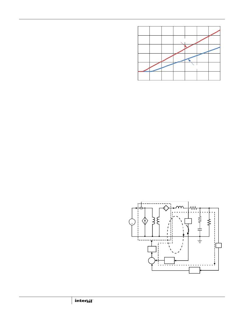
�FREQUENCY� (MHz)�
�FIGURE� 39.� MINIMUM� V� OUT� vs� FREQUENCY�
�Input� Capacitor� Selection�
�The� main� functions� for� the� input� capacitor� are� to� provide�
�decoupling� of� the� parasitic� inductance� and� to� provide� filtering�
�function� to� prevent� the� switching� current� flowing� back� to� the�
�battery� rail.� At� least� two� 22μF� X5R� or� X7R� ceramic� capacitors� are�
�a� good� starting� point� for� the� input� capacitor� selection.�
�Loop� Compensation� Design�
�When� there� is� an� external� resistor� connected� from� FS� to� SGND,�
�the� COMP� pin� is� active� for� external� loop� compensation.� The�
�ISL8016� uses� constant� frequency� peak� current� mode� control�
�architecture� to� achieve� fast� loop� transient� response.� An� accurate�
�current� sensing� pilot� device� in� parallel� with� the� upper� MOSFET� is�
�used� for� peak� current� control� signal� and� overcurrent� protection.�
�The� inductor� is� not� considered� as� a� state� variable� since� its� peak�
�current� is� constant,� and� the� system� becomes� single� order�
�system.� It� is� much� easier� to� design� a� type� II� compensator� to�
�stabilize� the� loop� than� to� implement� voltage� mode� control.� Peak�
�current� mode� control� has� inherent� input� voltage� feed-forward�
�function� to� achieve� good� line� regulation.� Figure� 40� shows� the�
�small� signal� model� of� the� synchronous� buck� regulator.�
�R� 2� =� R� 3� ?� ----------� –� 1� ?�
�V� O�
�?� VFB�
�?�
�I� IN�
�V� IN�
�I� Ld�
�V� INd�
�I� L�
�v� o�
�voltage� of� the� regulator.� The� value� for� the� feedback� resistor� is�
�typically� between� 10k� ?� and� 100k� ?� ,� as� shown� in� Equation� 5.�
�(EQ.� 5)�
�If� the� output� voltage� desired� is� 0.6V,� then� R� 3� is� left� unpopulated�
�and� R� 2� is� shorted.� There� is� a� leakage� current� from� VIN� to�
�PHASE.� It� is� recommended� to� preload� the� output� with� 10μA�
�+�
�^�
�^�
�^�
�1:D�
�^�
�^�
�L� P�
�RT�
�R� LP�
�Rc�
�Co�
�^�
�Ro�
�minimum.� Capacitance,� C� 3� ,� maybe� added� to� improve� transient�
�performance.� A� good� starting� point� for� C� 3� can� be� determined� by�
�choosing� a� value� that� provides� an� 80kHz� corner� frequency�
�with� R� 2� .�
�F� m�
�d� ^�
�T� i� (S)�
�K�
�VSET� marginally� adjusts� VFB� according� to� the� “Analog�
�V� COMP�
��Figure� 39� is� the� recommended� minimum� output� voltage� setting�
�vs� operational� frequency� in� order� to� avoid� the� minimum� On-Time�
�+�
�H� e� (S)�
�^�
�-Av(S)�
�T� V� (S)�
�specification.�
�FIGURE� 40.� SMALL� SIGNAL� MODEL� OF� SYNCHRONOUS� BUCK�
�REGULATOR�
�18�
�FN7616.1�
�May� 5,� 2011�
�相关PDF资料 |
PDF描述 |
|---|---|
| VE-B5W-EW-B1 | CONVERTER MOD DC/DC 5.5V 100W |
| VE-B50-EW-B1 | CONVERTER MOD DC/DC 5V 100W |
| VE-J4T-CY | CONVERTER MOD DC/DC 6.5V 50W |
| VE-B4W-EW-B1 | CONVERTER MOD DC/DC 5.5V 100W |
| VE-J4P-CY | CONVERTER MOD DC/DC 13.8V 50W |
相关代理商/技术参数 |
参数描述 |
|---|---|
| ISL8022 | 制造商:INTERSIL 制造商全称:Intersil Corporation 功能描述:Dual 2A/1.7A Low Quiescent Current 2.25MHz High Efficiency Synchronous |
| ISL8022EVAL1Z | 功能描述:EVAL BOARD 1 FOR ISL8022 RoHS:是 类别:编程器,开发系统 >> 评估板 - DC/DC 与 AC/DC(离线)SMPS 系列:* 产品培训模块:Obsolescence Mitigation Program 标准包装:1 系列:True Shutdown™ 主要目的:DC/DC,步升 输出及类型:1,非隔离 功率 - 输出:- 输出电压:- 电流 - 输出:1A 输入电压:2.5 V ~ 5.5 V 稳压器拓扑结构:升压 频率 - 开关:3MHz 板类型:完全填充 已供物品:板 已用 IC / 零件:MAX8969 |
| ISL8022EVAL2Z | 功能描述:EVAL BOARD 2 FOR ISL8023 RoHS:是 类别:编程器,开发系统 >> 评估板 - DC/DC 与 AC/DC(离线)SMPS 系列:* 产品培训模块:Obsolescence Mitigation Program 标准包装:1 系列:True Shutdown™ 主要目的:DC/DC,步升 输出及类型:1,非隔离 功率 - 输出:- 输出电压:- 电流 - 输出:1A 输入电压:2.5 V ~ 5.5 V 稳压器拓扑结构:升压 频率 - 开关:3MHz 板类型:完全填充 已供物品:板 已用 IC / 零件:MAX8969 |
| ISL8022IRZ | 功能描述:直流/直流开关调节器 DL CH 2 25MHZ 2 0 A & 1 7ASYNCHG 4X3 1 RoHS:否 制造商:International Rectifier 最大输入电压:21 V 开关频率:1.5 MHz 输出电压:0.5 V to 0.86 V 输出电流:4 A 输出端数量: 最大工作温度: 安装风格:SMD/SMT 封装 / 箱体:PQFN 4 x 5 |
| ISL8022IRZ-T | 功能描述:IC REG BUCK SYNC ADJ DL 12DFN RoHS:是 类别:集成电路 (IC) >> PMIC - 稳压器 - DC DC 开关稳压器 系列:- 产品培训模块:Lead (SnPb) Finish for COTS Obsolescence Mitigation Program 标准包装:2,500 系列:- 类型:降压(降压) 输出类型:两者兼有 输出数:1 输出电压:5V,1 V ~ 10 V 输入电压:3.5 V ~ 28 V PWM 型:电流模式 频率 - 开关:220kHz ~ 1MHz 电流 - 输出:600mA 同步整流器:无 工作温度:-40°C ~ 125°C 安装类型:表面贴装 封装/外壳:16-SSOP(0.154",3.90mm 宽) 包装:带卷 (TR) 供应商设备封装:16-QSOP |
发布紧急采购,3分钟左右您将得到回复。