- 您现在的位置:买卖IC网 > PDF目录13647 > ISL8023IRTAJZ (Intersil)IC VOLTAGE REGULATOR PDF资料下载
参数资料
| 型号: | ISL8023IRTAJZ |
| 厂商: | Intersil |
| 文件页数: | 14/20页 |
| 文件大小: | 0K |
| 描述: | IC VOLTAGE REGULATOR |
| 标准包装: | 100 |
| 系列: | * |
�� �
�
�ISL8023,� ISL8024�
�Theory� of� Operation�
�The� ISL8023,� ISL8024� is� a� step-down� switching� regulator�
�optimized� for� battery-powered� handheld� applications.� The�
�regulator� operates� at� 1MHz� fixed� default� switching� frequency,�
�when� FS� is� connected� to� VIN,� under� heavy� load� conditions� to�
�allow� smaller� external� inductors� and� capacitors� to� be� used� for�
�minimal� printed-circuit� board� (PCB)� area.� By� connecting� a�
�resistor� from� FS� to� SGND,� the� operational� frequency� adjustable�
�range� is� 500kHz� to� 4MHz.� At� light� load,� the� regulator� reduces� the�
�switching� frequency,� unless� forced� to� the� fixed� frequency,� to�
�minimize� the� switching� loss� and� to� maximize� the� battery� life.� The�
�quiescent� current� when� the� output� is� not� loaded� is� typically� only�
�50μA.� The� supply� current� is� typically� only� 5μA� when� the� regulator�
�is� shutdown.�
�PWM� Control� Scheme�
�Pulling� the� SYNC� pin� HI� (>0.8V)� forces� the� converter� into� PWM�
�mode,� regardless� of� output� current.� The� ISL8023,� ISL8024�
�employs� the� current-mode� pulse-width� modulation� (PWM)� control�
�scheme� for� fast� transient� response� and� pulse-by-pulse� current�
�limiting.� Figure� 3� on� page� 5� shows� the� Functional� Block� Diagram.�
�The� current� loop� consists� of� the� oscillator,� the� PWM� comparator,�
�current� sensing� circuit� and� the� slope� compensation� for� the�
�current� loop� stability.� The� slope� compensation� is� 440mV/Ts,�
�which� changes� with� frequency.� The� gain� for� the� current� sensing�
�circuit� is� typically� 200mV/A.� The� control� reference� for� the� current�
�loops� comes� from� the� error� amplifier's� (EAMP)� output.�
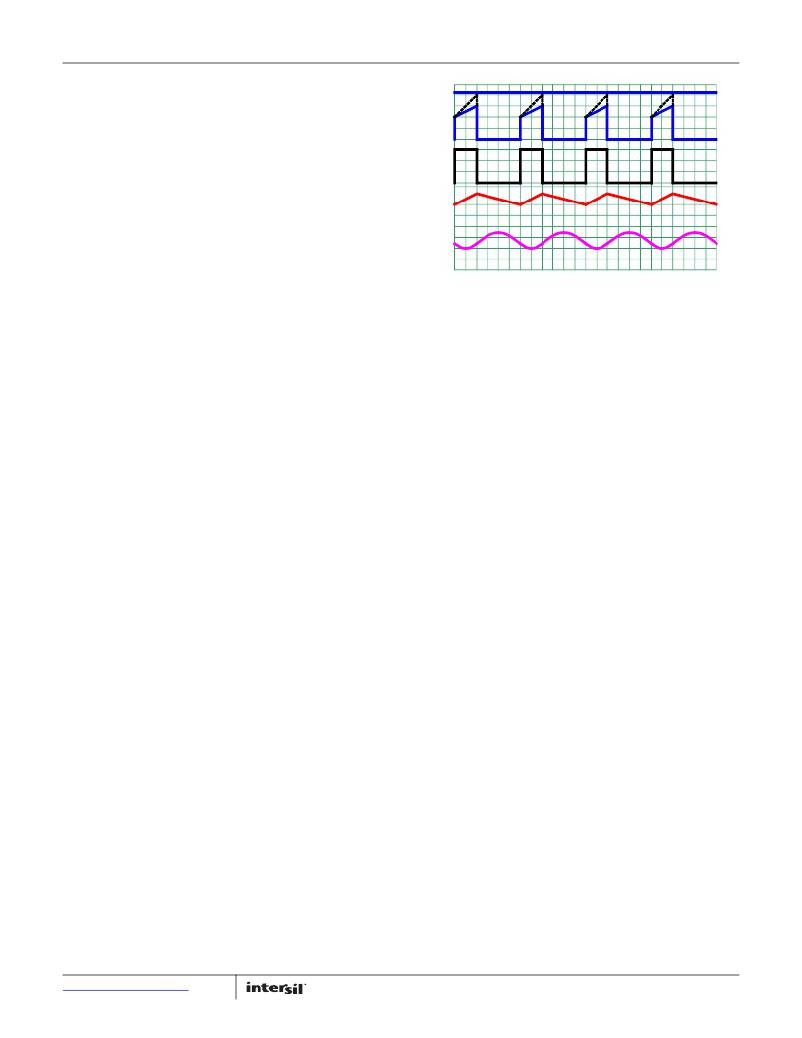
�The� PWM� operation� is� initialized� by� the� clock� from� the� oscillator.�
�The� P-Channel� MOSFET� is� turned� on� at� the� beginning� of� a� PWM�
�cycle� and� the� current� in� the� MOSFET� starts� to� ramp� up.� When� the�
�sum� of� the� current� amplifier� CSA� and� the� slope� compensation�
�reaches� the� control� reference� of� the� current� loop,� the� PWM�
�comparator� COMP� sends� a� signal� to� the� PWM� logic� to� turn� off� the�
�P-FET� and� turn� on� the� N-Channel� MOSFET.� The� N-FET� stays� on�
�until� the� end� of� the� PWM� cycle.� Figure� 39� shows� the� typical�
�operating� waveforms� during� the� PWM� operation.� The� dotted� lines�
�illustrate� the� sum� of� the� slope� compensation� ramp� and� the�
�current-sense� amplifier’s� CSA� output.�
�The� output� voltage� is� regulated� by� controlling� the� V� EAMP� voltage�
�to� the� current� loop.� The� bandgap� circuit� outputs� a� 0.6V� reference�
�voltage� to� the� voltage� loop.� The� feedback� signal� comes� from� the�
�VFB� pin.� The� soft-start� block� only� affects� the� operation� during� the�
�start-up� and� will� be� discussed� separately.� The� error� amplifier� is� a�
�transconductance� amplifier� that� converts� the� voltage� error� signal�
�to� a� current� output.� The� voltage� loop� is� internally� compensated�
�with� the� 55pF� and� 100k� ?� RC� network.� The� maximum� EAMP�
�voltage� output� is� precisely� clamped� to� 1.6V.�
�V� EAMP�
�V� CSA�
�DUTY�
�CYCLE�
�I� L�
�V� OUT�
�FIGURE� 39.� PWM� OPERATION� WAVEFORMS�
�SKIP� Mode�
�Pulling� the� SYNC� pin� LO� (<0.4V)� forces� the� converter� into� PFM�
�mode.� The� ISL8023,� ISL8024� enters� a� pulse-skipping� mode� at�
�light� load� to� minimize� the� switching� loss� by� reducing� the�
�switching� frequency.� Figure� 40� illustrates� the� skip-mode�
�operation.� A� zero-cross� sensing� circuit� shown� in� Figure� 3� on�
�page� 5� monitors� the� N-FET� current� for� zero� crossing.� When� 8�
�consecutive� cycles� of� the� inductor� current� crossing� zero� are�
�detected,� the� regulator� enters� the� skip� mode.� During� the� eight�
�detecting� cycles,� the� current� in� the� inductor� is� allowed� to� become�
�negative.� The� counter� is� reset� to� zero� when� the� current� in� any�
�cycle� does� not� cross� zero.�
�Once� the� skip� mode� is� entered,� the� pulse� modulation� starts� being�
�controlled� by� the� SKIP� comparator� shown� in� Figure� 3� on� page� 5.�
�Each� pulse� cycle� is� still� synchronized� by� the� PWM� clock.� The�
�P-FET� is� turned� on� at� the� clock's� rising� edge� and� turned� off� when�
�the� output� is� higher� than� 1.5%� of� the� nominal� regulation� or� when�
�its� current� reaches� the� peak� Skip� current� limit� value.� Then� the�
�inductor� current� is� discharging� to� 0A� and� stays� at� zero.� The�
�internal� clock� is� disabled.� The� output� voltage� reduces� gradually�
�due� to� the� load� current� discharging� the� output� capacitor.� When�
�the� output� voltage� drops� to� the� nominal� voltage,� the� P-FET� will� be�
�turned� on� again� at� the� rising� edge� of� the� internal� clock� as� it�
�repeats� the� previous� operations.�
�The� regulator� resumes� normal� PWM� mode� operation� when� the�
�output� voltage� drops� 1.5%� below� the� nominal� voltage.�
��14�
�FN7812.3�
�March� 24,� 2014�
�相关PDF资料 |
PDF描述 |
|---|---|
| GEM36DTMT | CONN EDGECARD 72POS R/A .156 SLD |
| GCM30DTMI | CONN EDGECARD 60POS R/A .156 SLD |
| GMM18DSUS | CONN EDGECARD 36POS DIP .156 SLD |
| GCM30DTBI | CONN EDGECARD 60POS R/A .156 SLD |
| GSM18DSUS | CONN EDGECARD 36POS DIP .156 SLD |
相关代理商/技术参数 |
参数描述 |
|---|---|
| ISL8023IRTAJZ-T | 功能描述:IC VOLTAGE REGULATOR RoHS:是 类别:集成电路 (IC) >> PMIC - 稳压器 - DC DC 开关稳压器 系列:* 产品培训模块:Lead (SnPb) Finish for COTS Obsolescence Mitigation Program 标准包装:2,500 系列:- 类型:降压(降压) 输出类型:两者兼有 输出数:1 输出电压:5V,1 V ~ 10 V 输入电压:3.5 V ~ 28 V PWM 型:电流模式 频率 - 开关:220kHz ~ 1MHz 电流 - 输出:600mA 同步整流器:无 工作温度:-40°C ~ 125°C 安装类型:表面贴装 封装/外壳:16-SSOP(0.154",3.90mm 宽) 包装:带卷 (TR) 供应商设备封装:16-QSOP |
| ISL8023IRTAJZ-T7 | 功能描述:直流/直流开关转换器 3A, Adjustable Vout, Low Quiescent Current Synch. Buck Regul RoHS:否 制造商:STMicroelectronics 最大输入电压:4.5 V 开关频率:1.5 MHz 输出电压:4.6 V 输出电流:250 mA 输出端数量:2 最大工作温度:+ 85 C 安装风格:SMD/SMT |
| ISL8023IRTAJZ-T7A | 功能描述:直流/直流开关转换器 3A ADJ VOUT LW QUIES CENT CUR SYNC BUCK RoHS:否 制造商:STMicroelectronics 最大输入电压:4.5 V 开关频率:1.5 MHz 输出电压:4.6 V 输出电流:250 mA 输出端数量:2 最大工作温度:+ 85 C 安装风格:SMD/SMT |
| ISL8024 | 制造商:INTERSIL 制造商全称:Intersil Corporation 功能描述:3A/4A Low Quiescent Current High Efficiency Synchronous Buck Regulator |
| ISL8024AEVAL3Z | 制造商:Intersil Corporation 功能描述:ISL8024A EVALUATION BOARD 3 - ROHS COMPLIANT - 16 LEAD - - Bulk |
发布紧急采购,3分钟左右您将得到回复。