- 您现在的位置:买卖IC网 > PDF目录15209 > ISL8104CBZ-T (Intersil)IC REG CTRLR BUCK PWM VM 14-SOIC PDF资料下载
参数资料
| 型号: | ISL8104CBZ-T |
| 厂商: | Intersil |
| 文件页数: | 8/14页 |
| 文件大小: | 0K |
| 描述: | IC REG CTRLR BUCK PWM VM 14-SOIC |
| 标准包装: | 2,500 |
| PWM 型: | 电压模式 |
| 输出数: | 1 |
| 频率 - 最大: | 1.5MHz |
| 占空比: | 100% |
| 电源电压: | 7.6 V ~ 15.4 V |
| 降压: | 是 |
| 升压: | 无 |
| 回扫: | 无 |
| 反相: | 无 |
| 倍增器: | 无 |
| 除法器: | 无 |
| Cuk: | 无 |
| 隔离: | 无 |
| 工作温度: | 0°C ~ 70°C |
| 封装/外壳: | 14-SOIC(0.154",3.90mm 宽) |
| 包装: | 带卷 (TR) |
�� �
�
�ISL8104�
�will� repeat� this� process� in� a� hiccup� mode.� Figure� 4� shows� a�
�typical� reaction� to� a� repeated� overcurrent� condition� that�
�places� the� regulator� in� a� hiccup� mode.� If� the� regulator� is�
�repeatedly� tripping� overcurrent,� the� hiccup� period� can� be�
�approximated� by� Equation� 5:�
�temperature� range.� System� Accuracy� includes� Error� Amplifier�
�offset,� and� Reference� Error.� The� use� of� REFIN� may� add� up� to�
�3mV� of� offset� error� into� the� system� (as� the� Error� Amplifier�
�offset� is� trimmed� out� via� the� internal� System� reference).�
�t� HICCUP� =� --------------------------------�
�2� ?� 4V� ?� C� SS�
�30� μ� A�
�(EQ.� 5)�
�Application� Guidelines�
�Layout� Considerations�
�The� OCP� trip� point� varies� mainly� due� to� MOSFET� r� DS(ON)�
�variations� and� layout� noise� concerns.� To� avoid� overcurrent�
�tripping� in� the� normal� operating� load� range,� find� the� R� OCSET�
�resistor� from� the� following� equations� with:�
�1.� The� maximum� r� DS(ON)� at� the� highest� junction�
�temperature�
�2.� The� minimum� I� TSOC� from� the� specification� table�
�Determine� the� overcurrent� trip� point� greater� than� the�
�As� in� any� high� frequency� switching� converter,� layout� is� very�
�important.� Switching� current� from� one� power� device� to� another�
�can� generate� voltage� transients� across� the� impedances� of� the�
�interconnecting� bond� wires� and� circuit� traces.� These�
�interconnecting� impedances� should� be� minimized� by� using�
�wide,� short� printed� circuit� traces.� The� critical� components�
�should� be� located� as� close� together� as� possible� using� ground�
�plane� construction� or� single� point� grounding.�
�R� TSOC� =� ----------------------------------------------------------------�
�maximum� output� continuous� current� at� maximum� inductor�
�ripple� current.�
�SIMPLE� OCP� EQUATION�
�I� OC_SOURCE� ?� r� DS� (� ON� )�
�200� μ� A�
�DETAILED� OCP� EQUATION�
�VCC�
�PVCC�
�ISL8104�
�+14V�
�C� BP_PVCC�
�C� BP_VCC�
�VIN�
�?� I�
�+� -----� ?� ?� r�
�----------------------------------------------------------------------------------� )�
�?� OC_SOURCE� 2� ?�
�R� TSOC� =�
�Δ� I�
�I� TSOC� ?� N� T�
�DS� (� ON�
�TGATE�
�BOOT�
�Q� 1�
�C� IN�
�V� IN� -� V� OUT� V� OUT�
�f� SW� ?� L� OUT�
�N� T� = NUMBER OF TOP-SIDE MOSFETs�
�Δ� I� =� --------------------------------� ?� ----------------�
�V� IN�
�f� SW� =� Regulator� Switching� Frequency�
�(EQ.� 6)�
�LX�
�C� IN�
�L� OUT�
�C� OUT�
�V� OUT�
�High� Speed� MOSFET� Gate� Driver�
�BGATE�
�Q� 2�
���GND�
�SS�
�PGND�
�C� SS�
��������Reference� Input�
�The� REFIN� pin� allows� the� user� to� bypass� the� internal� 0.597V�
�reference� with� an� external� reference.� If� REFIN� is� NOT� above�
�~2.2V,� the� external� reference� pin� is� used� as� the� control�
�reference� instead� of� the� internal� 0.597V� reference.� When� not�
�using� the� external� reference� option,� the� REFIN� pin� should� be�
�left� floating.� An� internal� 6μA� pull-up� keeps� this� REFIN� pin�
�above� 2.2V� in� this� situation.�
�Internal� Reference� and� System� Accuracy�
�The� Internal� Reference� is� set� to� 0.597V.� The� total� DC� system�
�accuracy� of� the� system� is� to� be� within� 1.5%� over� the� industrial�
�8�
�KEY�
�TRACE� SIZED� FOR� 3A� PEAK� CURRENT�
�SHORT� TRACE,� MINIMUM� IMPEDANCE�
�ISLAND� ON� POWER� PLANE� LAYER�
�ISLAND� ON� CIRCUIT� AND/OR� POWER� PLANE� LAYER�
�VIA� CONNECTION� TO� GROUND� PLANE�
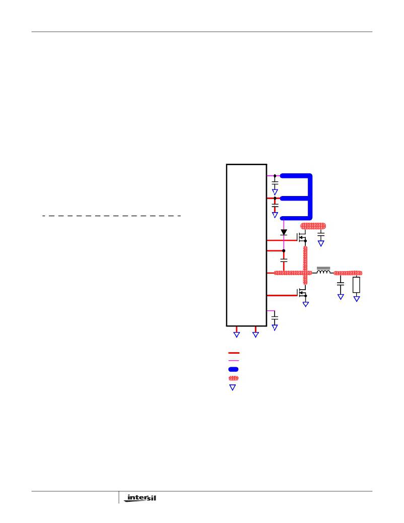
�FIGURE� 5.� PRINTED� CIRCUIT� BOARD� POWER� PLANES�
�AND� ISLANDS�
�A� multi-layer� printed� circuit� board� is� recommended.� Figure� 5�
�shows� the� critical� components� of� the� converter.� Note� that�
�capacitors� C� IN� and� C� OUT� could� each� represent� numerous�
�physical� capacitors.� Dedicate� one� solid� layer� (usually� a� middle�
�layer� of� the� PC� board)� for� a� ground� plane� and� make� all� critical�
�component� ground� connections� with� vias� to� this� layer.�
�Dedicate� another� solid� layer� as� a� power� plane� and� break� this�
�plane� into� smaller� islands� of� common� voltage� levels.� Keep� the�
�metal� runs� from� the� LX� terminals� to� the� output� inductor� short.�
�FN9257.2�
�March� 7,� 2008�
�相关PDF资料 |
PDF描述 |
|---|---|
| ISL8104CRZ-T | IC REG CTRLR BUCK PWM VM 16-QFN |
| VI-B7Y-EY-F3 | CONVERTER MOD DC/DC 3.3V 33W |
| CAT812TTBI-T3 | IC SUPERVISOR MPU 3.08V SOT143-4 |
| ISL6535CBZ-T | IC REG CTRLR BUCK PWM VM 14-SOIC |
| ISL6535IBZ-T | IC REG CTRLR BUCK PWM VM 14-SOIC |
相关代理商/技术参数 |
参数描述 |
|---|---|
| ISL8104CRZ | 功能描述:IC REG CTRLR BUCK PWM VM 16-QFN RoHS:是 类别:集成电路 (IC) >> PMIC - 稳压器 - DC DC 切换控制器 系列:- 产品培训模块:Lead (SnPb) Finish for COTS Obsolescence Mitigation Program 标准包装:2,500 系列:- PWM 型:电流模式 输出数:1 频率 - 最大:275kHz 占空比:50% 电源电压:18 V ~ 110 V 降压:无 升压:无 回扫:无 反相:无 倍增器:无 除法器:无 Cuk:无 隔离:是 工作温度:-40°C ~ 85°C 封装/外壳:8-SOIC(0.154",3.90mm 宽) 包装:带卷 (TR) |
| ISL8104CRZ-T | 功能描述:IC REG CTRLR BUCK PWM VM 16-QFN RoHS:是 类别:集成电路 (IC) >> PMIC - 稳压器 - DC DC 切换控制器 系列:- 产品培训模块:Lead (SnPb) Finish for COTS Obsolescence Mitigation Program 标准包装:2,500 系列:- PWM 型:电流模式 输出数:1 频率 - 最大:275kHz 占空比:50% 电源电压:18 V ~ 110 V 降压:无 升压:无 回扫:无 反相:无 倍增器:无 除法器:无 Cuk:无 隔离:是 工作温度:-40°C ~ 85°C 封装/外壳:8-SOIC(0.154",3.90mm 宽) 包装:带卷 (TR) |
| ISL8104EVAL1Z | 功能描述:EVALUATION BOARD FOR ISL8104 RoHS:是 类别:编程器,开发系统 >> 评估板 - DC/DC 与 AC/DC(离线)SMPS 系列:- 产品培训模块:Obsolescence Mitigation Program 标准包装:1 系列:True Shutdown™ 主要目的:DC/DC,步升 输出及类型:1,非隔离 功率 - 输出:- 输出电压:- 电流 - 输出:1A 输入电压:2.5 V ~ 5.5 V 稳压器拓扑结构:升压 频率 - 开关:3MHz 板类型:完全填充 已供物品:板 已用 IC / 零件:MAX8969 |
| ISL8104EVAL2Z | 功能描述:EVAL BOARD 2 FOR ISL8104 RoHS:是 类别:编程器,开发系统 >> 评估板 - DC/DC 与 AC/DC(离线)SMPS 系列:* 标准包装:1 系列:- 主要目的:DC/DC,步降 输出及类型:1,非隔离 功率 - 输出:- 输出电压:3.3V 电流 - 输出:3A 输入电压:4.5 V ~ 28 V 稳压器拓扑结构:降压 频率 - 开关:250kHz 板类型:完全填充 已供物品:板 已用 IC / 零件:L7981 其它名称:497-12113STEVAL-ISA094V1-ND |
| ISL8104IBZ | 功能描述:IC REG CTRLR BUCK PWM VM 14-SOIC RoHS:是 类别:集成电路 (IC) >> PMIC - 稳压器 - DC DC 切换控制器 系列:- 产品培训模块:Lead (SnPb) Finish for COTS Obsolescence Mitigation Program 标准包装:2,500 系列:- PWM 型:电流模式 输出数:1 频率 - 最大:275kHz 占空比:50% 电源电压:18 V ~ 110 V 降压:无 升压:无 回扫:无 反相:无 倍增器:无 除法器:无 Cuk:无 隔离:是 工作温度:-40°C ~ 85°C 封装/外壳:8-SOIC(0.154",3.90mm 宽) 包装:带卷 (TR) |
发布紧急采购,3分钟左右您将得到回复。