- 您现在的位置:买卖IC网 > PDF目录15217 > ISL8105BCRZ-T (Intersil)IC REG CTRLR BUCK PWM VM 10-DFN PDF资料下载
参数资料
| 型号: | ISL8105BCRZ-T |
| 厂商: | Intersil |
| 文件页数: | 11/16页 |
| 文件大小: | 0K |
| 描述: | IC REG CTRLR BUCK PWM VM 10-DFN |
| 标准包装: | 6,000 |
| PWM 型: | 电压模式 |
| 输出数: | 1 |
| 频率 - 最大: | 330kHz |
| 占空比: | 100% |
| 电源电压: | 6.5 V ~ 14.4 V |
| 降压: | 是 |
| 升压: | 无 |
| 回扫: | 无 |
| 反相: | 无 |
| 倍增器: | 无 |
| 除法器: | 无 |
| Cuk: | 无 |
| 隔离: | 无 |
| 工作温度: | 0°C ~ 70°C |
| 封装/外壳: | 10-VFDFN 裸露焊盘 |
| 包装: | 带卷 (TR) |
�� �
�
�ISL8105B�
�earlier.� Locate� the� capacitor,� C� BOOT� ,� as� close� as� practical� to�
�the� BOOT� and� LX� pins.� All� components� used� for� feedback�
�For� the� purpose� of� this� analysis,� C� and� ESR� represent� the� total�
�output� capacitance� and� its� equivalent� series� resistance.�
�F� LC� =� ---------------------------�
�F� CE� =� ---------------------------------�
�compensation� (not� shown)� should� be� located� as� close� to� the�
�IC� as� practical.�
�1�
�2� π� ?� L� ?� C�
�1�
�2� π� ?� C� ?� ESR�
�(EQ.� 4)�
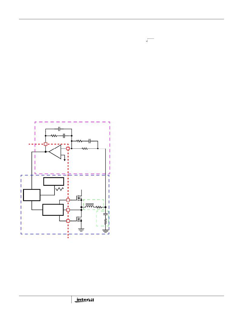
�Feedback� Compensation�
�This� section� highlights� the� design� considerations� for� a�
�voltage-mode� controller� requiring� external� compensation.� To�
�address� a� broad� range� of� applications,� a� type-3� feedback�
�network� is� recommended� (see� Figure� 9).�
�Figure� 9� highlights� the� voltage-mode� control� loop� for� a�
�synchronous-rectified� buck� converter,� applicable� to� the�
�ISL805B� circuit.� The� output� voltage� (V� OUT� )� is� regulated� to�
�the� reference� voltage,� V� REF� ,� level.� The� error� amplifier� output�
�(COMP� pin� voltage)� is� compared� with� the� oscillator� (OSC)�
�triangle� wave� to� provide� a� pulse-width� modulated� wave� with�
�an� amplitude� of� V� IN� at� the� LX� node.� The� PWM� wave� is�
�smoothed� by� the� output� filter� (L� and� C).� The� output� filter�
�capacitor� bank’s� equivalent� series� resistance� is� represented�
�by� the� series� resistor� ESR.�
�The� compensation� network� consists� of� the� error� amplifier�
�(internal� to� the� ISL8105B)� and� the� external� R� 1� to� R� 3� ,� C� 1� to� C� 3�
�components.� The� goal� of� the� compensation� network� is� to�
�provide� a� closed� loop� transfer� function� with� high� 0dB� crossing�
�frequency� (F� 0� ;� typically� 0.1� to� 0.3� of� f� SW� )� and� adequate� phase�
�margin� (better� than� +45°).� Phase� margin� is� the� difference�
�between� the� closed� loop� phase� at� F� 0dB� and� +180°.� The�
�equations� that� follow� relate� the� compensation� network’s� poles,�
�zeros� and� gain� to� the� components� (R� 1� ,� R� 2� ,� R� 3� ,� C� 1� ,� C� 2� ,� and�
�C� 3� )� in� Figure� 9.� Use� the� following� guidelines� for� locating� the�
�poles� and� zeros� of� the� compensation� network:�
�1.� Select� a� value� for� R� 1� (1k� Ω� to� 10k� Ω� ,� typically).� Calculate�
�value� for� R� 2� for� desired� converter� bandwidth� (F� 0� ).� If�
�setting� the� output� voltage� to� be� equal� to� the� reference� set�
�voltage� as� shown� in� Figure� 9,� the� design� procedure� is�
�d� MAX� ?� V� IN� ?� F� LC�
�COMP�
�R� 2�
�E/A�
�C� 2�
�-�
�+�
�C� 1�
�FB�
�R� 3�
�R� 1�
�C� 3�
�shown� in� Equation� 5.�
�V� OSC� ?� R� 1� ?� F� 0�
�R� 2� =� ---------------------------------------------� (EQ.� 5)�
�2.� Calculate� C� 1� such� that� F� Z1� is� placed� at� a� fraction� of� the� F� LC� ,�
�at� 0.1� to� 0.75� of� F� LC� (to� adjust,� change� the� 0.5� factor� to�
�desired� number).� The� higher� the� quality� factor� of� the� output�
�filter� and/or� the� higher� the� ratio� F� CE� /F� LC� ,� the� lower� the� F� Z1�
�frequency� (to� maximize� phase� boost� at� F� LC� ).�
�C� 1� =� -----------------------------------------------�
�VREF�
�1�
�2� π� ?� R� 2� ?� 0.5� ?� F� LC�
�3.� Calculate� C� 2� such� that� F� P1� is� placed� at� F� CE� .�
�(EQ.� 6)�
�2� π� ?� R� 2� ?� C� 1� ?� F� CE� –� 1�
�OSCILLATOR�
�V� IN�
�V� OUT�
�C� 1�
�C� 2� =� --------------------------------------------------------�
�(EQ.� 7)�
�PWM�
�CIRCUIT�
�V� OSC�
�HALF-BRIDGE�
�DRIVE�
�TGATE�
�LX�
�L�
�DCR�
�C�
�4.� Calculate� R� 3� such� that� F� Z2� is� placed� at� F� LC� .� Calculate� C� 3�
�such� that� F� P2� is� placed� below� F� SW� (typically,� 0.5� to� 1.0�
�times� F� SW� ).� F� SW� represents� the� regulator� ’s� switching�
�frequency.� Change� the� numerical� factor� to� reflect� desired�
�placement� of� this� pole.� Placement� of� F� P2� lower� in�
�frequency� helps� reduce� the� gain� of� the� compensation�
�network� at� high� frequency,� in� turn� reducing� the� HF� ripple�
�BGATE�
�ESR�
�component� at� the� COMP� pin� and� minimizing� resultant�
�duty� cycle� jitter.�
�F� SW�
�F� LC�
�C� 3� =� -------------------------------------------------�
�ISL8105B� EXTERNAL� CIRCUIT�
�FIGURE� 9.� VOLTAGE-MODE� BUCK� CONVERTER�
�COMPENSATION� DESIGN�
�R� 1�
�R� 3� =� ----------------------�
�------------� –� 1�
�1�
�2� π� ?� R� 3� ?� 0.7� ?� F� SW�
�(EQ.� 8)�
�The� modulator� transfer� function� is� the� small-signal� transfer�
�function� of� V� OUT� /V� COMP� .� This� function� is� dominated� by� a� DC�
�gain,� given� by� d� MAX� V� IN� /V� OSC� ,� and� shaped� by� the� output� filter,�
�with� a� double� pole� break� frequency� at� F� LC� and� a� zero� at� F� CE� .�
�11�
�It� is� recommended� that� a� mathematical� model� is� used� to� plot�
�the� loop� response.� Check� the� loop� gain� against� the� error�
�amplifier� ’s� open-loop� gain.� Verify� phase� margin� results� and�
�adjust� as� necessary.� Equations� 9� and� 10� describe� the�
�frequency� response� of� the� modulator� (G� MOD� ),� feedback�
�compensation� (G� FB� )� and� closed-loop� response� (G� CL� ):�
�FN6447.2�
�April� 15,� 2010�
�相关PDF资料 |
PDF描述 |
|---|---|
| CAT8801TSD-GT3 | IC SUPERVISOR 3.075V SC-70-3 |
| ISL8105ACRZ-T | IC REG CTRLR BUCK PWM VM 10-DFN |
| CAT8801LTB-GT3 | IC SUPERVISOR 4.625V SOT-23-3 |
| CAT8801LSD-GT3 | IC SUPERVISOR 4.625V SC-70-3 |
| CAT8801TTB-GT3 | VOLTAGE SUP LOW CURRENT |
相关代理商/技术参数 |
参数描述 |
|---|---|
| ISL8105BEVAL1Z | 功能描述:EVAL BOARD ISL8105B RoHS:是 类别:编程器,开发系统 >> 评估板 - DC/DC 与 AC/DC(离线)SMPS 系列:- 产品培训模块:Obsolescence Mitigation Program 标准包装:1 系列:True Shutdown™ 主要目的:DC/DC,步升 输出及类型:1,非隔离 功率 - 输出:- 输出电压:- 电流 - 输出:1A 输入电压:2.5 V ~ 5.5 V 稳压器拓扑结构:升压 频率 - 开关:3MHz 板类型:完全填充 已供物品:板 已用 IC / 零件:MAX8969 |
| ISL8105BEVAL2Z | 功能描述:EVALUATION BOARD FOR ISL8105B RoHS:是 类别:编程器,开发系统 >> 评估板 - DC/DC 与 AC/DC(离线)SMPS 系列:- 产品培训模块:Obsolescence Mitigation Program 标准包装:1 系列:True Shutdown™ 主要目的:DC/DC,步升 输出及类型:1,非隔离 功率 - 输出:- 输出电压:- 电流 - 输出:1A 输入电压:2.5 V ~ 5.5 V 稳压器拓扑结构:升压 频率 - 开关:3MHz 板类型:完全填充 已供物品:板 已用 IC / 零件:MAX8969 |
| ISL8105BIBZ | 功能描述:IC REG CTRLR BUCK PWM VM 8-SOIC RoHS:是 类别:集成电路 (IC) >> PMIC - 稳压器 - DC DC 切换控制器 系列:- 产品培训模块:Lead (SnPb) Finish for COTS Obsolescence Mitigation Program 标准包装:2,500 系列:- PWM 型:电流模式 输出数:1 频率 - 最大:275kHz 占空比:50% 电源电压:18 V ~ 110 V 降压:无 升压:无 回扫:无 反相:无 倍增器:无 除法器:无 Cuk:无 隔离:是 工作温度:-40°C ~ 85°C 封装/外壳:8-SOIC(0.154",3.90mm 宽) 包装:带卷 (TR) |
| ISL8105BIBZ-T | 功能描述:IC REG CTRLR BUCK PWM VM 8-SOIC RoHS:是 类别:集成电路 (IC) >> PMIC - 稳压器 - DC DC 切换控制器 系列:- 产品培训模块:Lead (SnPb) Finish for COTS Obsolescence Mitigation Program 标准包装:2,500 系列:- PWM 型:电流模式 输出数:1 频率 - 最大:275kHz 占空比:50% 电源电压:18 V ~ 110 V 降压:无 升压:无 回扫:无 反相:无 倍增器:无 除法器:无 Cuk:无 隔离:是 工作温度:-40°C ~ 85°C 封装/外壳:8-SOIC(0.154",3.90mm 宽) 包装:带卷 (TR) |
| ISL8105BIRZ | 功能描述:IC REG CTRLR BUCK PWM VM 10-DFN RoHS:是 类别:集成电路 (IC) >> PMIC - 稳压器 - DC DC 切换控制器 系列:- 产品培训模块:Lead (SnPb) Finish for COTS Obsolescence Mitigation Program 标准包装:2,500 系列:- PWM 型:电流模式 输出数:1 频率 - 最大:275kHz 占空比:50% 电源电压:18 V ~ 110 V 降压:无 升压:无 回扫:无 反相:无 倍增器:无 除法器:无 Cuk:无 隔离:是 工作温度:-40°C ~ 85°C 封装/外壳:8-SOIC(0.154",3.90mm 宽) 包装:带卷 (TR) |
发布紧急采购,3分钟左右您将得到回复。