参数资料
| 型号: | ISL83385EIB-T |
| 厂商: | Intersil |
| 文件页数: | 8/11页 |
| 文件大小: | 0K |
| 描述: | IC 2DRVR/2RCVR RS232 3V 18-SOIC |
| 标准包装: | 1,000 |
| 类型: | 收发器 |
| 驱动器/接收器数: | 2/2 |
| 规程: | RS232 |
| 电源电压: | 3 V ~ 5.5 V |
| 安装类型: | 表面贴装 |
| 封装/外壳: | 18-SOIC(0.295",7.50mm 宽) |
| 供应商设备封装: | 18-SOIC W |
| 包装: | 带卷 (TR) |

6
FN6001.4
January 16, 2005
hysteresis to increase noise immunity and decrease errors
due to slow input signal transitions.
Low Power Operation
This 3V device requires a nominal supply current of 0.3mA,
even at VCC = 5.5V, during normal operation (not in
powerdown mode). This is considerably less than the 11mA
current required by comparable 5V RS-232 devices, allowing
users to reduce system power simply by replacing the old
style device with the ISL83385E in new designs.
Powerdown Functionality
The already low current requirement drops significantly
when the device enters powerdown mode. In powerdown,
supply current drops to 1
A, because the on-chip charge
pump turns off (V+ collapses to VCC, V- collapses to GND),
and the transmitter outputs three-state. This micro-power
mode makes these devices ideal for battery powered and
portable applications.
Software Controlled (Manual) Powerdown
The ISL83385E may be forced into its low power, standby
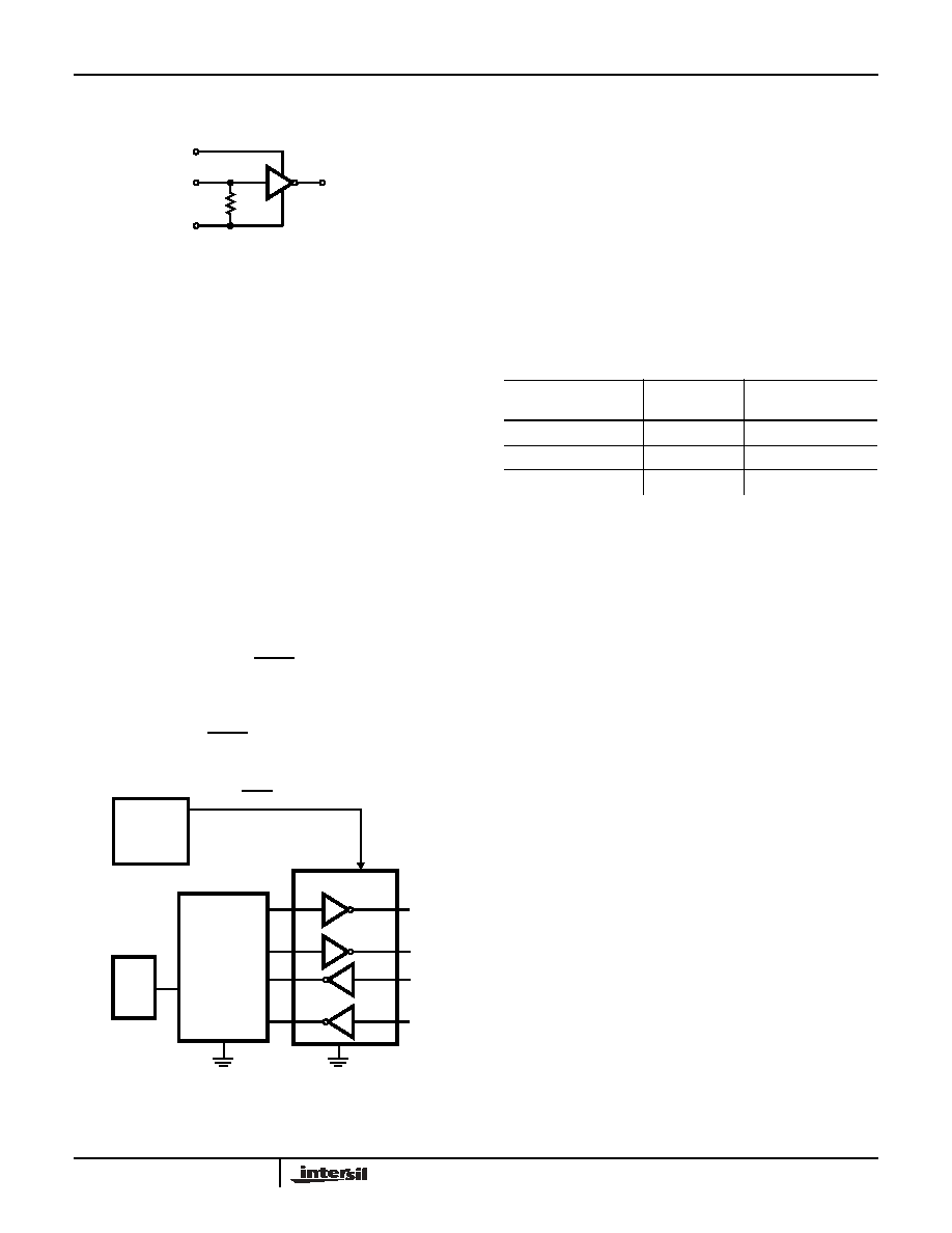
state via a simple shutdown (SHDN) pin (see Figure 2).
Driving this pin high enables normal operation, while driving
it low forces the IC into it’s powerdown state. The time
required to exit powerdown, and resume transmission is less
than 100
s. Connect SHDN to VCC if the powerdown
function isn’t needed.
Capacitor Selection
These charge pumps only require 0.1
F capacitors for the
full operational voltage range. Table 3 lists other acceptable
capacitor values for various supply voltage ranges. Do not
use values smaller than those listed in Table 3. Increasing
the capacitor values (by a factor of 2) reduces ripple on the
transmitter outputs and slightly reduces power consumption.
When using minimum required capacitor values, make sure
that capacitor values do not degrade excessively with
temperature. If in doubt, use capacitors with a larger nominal
value. The capacitor’s equivalent series resistance (ESR)
usually rises at low temperatures and it influences the
amount of ripple on V+ and V-.
Power Supply Decoupling
In most circumstances a 0.1
F bypass capacitor is
adequate. In applications that are particularly sensitive to
power supply noise, decouple VCC to ground with a
capacitor of the same value as the charge-pump capacitor C1.
Connect the bypass capacitor as close as possible to the IC.
Operation Down to 2.7V
ISL83385E transmitter outputs meet RS-562 levels (±3.7V),
at the full data rate, with VCC as low as 2.7V. RS-562 levels
typically ensure inter operability with RS-232 devices.
Transmitter Outputs when Exiting
Powerdown
Figure 3 shows the response of two transmitter outputs
when exiting powerdown mode. As they activate, the two
transmitter outputs properly go to opposite RS-232 levels,
with no glitching, ringing, nor undesirable transients. Each
transmitter is loaded with 3k
in parallel with 2500pF. Note
that the transmitters enable only when the magnitude of the
supplies exceed approximately 3V.
RXOUT
GND
≤ VROUT ≤ VCC
5k
RXIN
-25V
≤ VRIN ≤ +25V
GND
VCC
FIGURE 1. INVERTING RECEIVER CONNECTIONS
FIGURE 2. CONNECTIONS FOR MANUAL POWERDOWN
PWR
SHDN
CPU
I/O
ISL83385E
MGT
LOGIC
UART
TABLE 3. REQUIRED CAPACITOR VALUES
VCC
(V)
C1
(
F)
C2, C3, C4
(
F)
3.0 to 3.6
0.1
4.5 to 5.5
0.047
0.33
3.0 to 5.5
0.1
0.47
ISL83385E
相关PDF资料 |
PDF描述 |
|---|---|
| ISL83386EIV-T | IC 3DRVR/2RCVR RS232 3V 20-TSSOP |
| ISL83387EIV-T | IC 3DRVR/3RCVR RS232 3V 24-TSSOP |
| ISL83491IP | IC TXRX RS485/422 3.3V LP 14-DIP |
| ISL98002CRZ-170 | IC VID DIGITIZER 3CHN AFE 72-QFN |
| ISL98003CNZ-165 | IC AFE 3CH 8BIT 165MHZ 80EPTQFP |
相关代理商/技术参数 |
参数描述 |
|---|---|
| ISL83385EIBZ | 功能描述:IC 2DRVR/2RCVR RS232 18-SOIC RoHS:是 类别:集成电路 (IC) >> 接口 - 驱动器,接收器,收发器 系列:- 产品培训模块:Lead (SnPb) Finish for COTS Obsolescence Mitigation Program 标准包装:2,500 系列:- 类型:发射器 驱动器/接收器数:4/0 规程:RS422,RS485 电源电压:4.75 V ~ 5.25 V 安装类型:表面贴装 封装/外壳:16-SOIC(0.154",3.90mm 宽) 供应商设备封装:16-SOIC 包装:带卷 (TR) |
| ISL83385EIBZ-T | 功能描述:IC 2DRVR/2RCVR RS232 18-SOIC RoHS:是 类别:集成电路 (IC) >> 接口 - 驱动器,接收器,收发器 系列:- 标准包装:250 系列:- 类型:收发器 驱动器/接收器数:2/2 规程:RS232 电源电压:3 V ~ 5.5 V 安装类型:表面贴装 封装/外壳:16-TSSOP(0.173",4.40mm 宽) 供应商设备封装:16-TSSOP 包装:带卷 (TR) |
| ISL83385IA | 制造商:Rochester Electronics LLC 功能描述:- Bulk 制造商:Harris Corporation 功能描述: |
| ISL83386E | 制造商:INTERSIL 制造商全称:Intersil Corporation 功能描述:【15kV ESD Protected, +3V to +5.5V, 1 Microamp, 250kbps, RS-232 Transmitters/Receivers with Separate Logic Supply |
| ISL83386E_04 | 制造商:INTERSIL 制造商全称:Intersil Corporation 功能描述:【15kV ESD Protected, +3V to +5.5V, 1 Microamp, 250kbps, RS-232 Transmitters/Receivers with Separate Logic Supply |
发布紧急采购,3分钟左右您将得到回复。