参数资料
| 型号: | ISL8394IB-T |
| 厂商: | Intersil |
| 文件页数: | 10/11页 |
| 文件大小: | 0K |
| 描述: | IC SWITCH QUAD SPDT 20SOIC |
| 标准包装: | 1,000 |
| 功能: | 开关 |
| 电路: | 4 x SPDT |
| 导通状态电阻: | 35 欧姆 |
| 电压电源: | 单/双电源 |
| 电压 - 电源,单路/双路(±): | 2 V ~ 12 V,±2 V ~ 6 V |
| 电流 - 电源: | 10nA |
| 工作温度: | -40°C ~ 85°C |
| 安装类型: | 表面贴装 |
| 封装/外壳: | 20-SOIC(0.295",7.50mm 宽) |
| 供应商设备封装: | 20-SOIC W |
| 包装: | 带卷 (TR) |
8
FN6038.3
March 13, 2006
1V above V-. The low leakage current performance is
unaffected by this approach, but the switch resistance may
increase, especially at low supply voltages.
Power-Supply Considerations
The ISL8394 construction is typical of most CMOS analog
switches, in that they have three supply pins: V+, V-, and
GND. V+ and V- drive the internal CMOS switches and set
their analog voltage limits, so there are no connections
between the analog signal path and GND. Unlike switches
with a 13V maximum supply voltage, the ISL8394 15V
maximum supply voltage provides plenty of room for the
10% tolerance of 12V supplies (±6V or 12V single supply),
as well as room for overshoot and noise spikes.
This family of switches performs equally well when operated
with bipolar or single voltage supplies.The minimum
recommended supply voltage is 2V or ±2V. It is important to
note that the input signal range, switching times, and on-
resistance degrade at lower supply voltages. Refer to the
electrical specification tables and Typical Performance
curves for details.
V+ and GND power the internal logic (thus setting the digital
switching point) and level shifters. The level shifters convert
the logic levels to switched V+ and V- signals to drive the
analog switch gate terminals.
Logic-Level Thresholds
V+ and GND power the internal logic stages, so V- has no
affect on logic thresholds. This switch family is TTL
compatible (0.8V and 2.4V) over a V+ supply range of 2.7V
to 10V. At 12V the VIH level is about 2.5V. This is still below
the TTL guaranteed high output minimum level of 2.8V, but
noise margin is reduced. For best results with a 12V supply,
use a logic family that provides a VOH greater than 3V.
The digital input stages draw supply current whenever the
digital input voltage is not at one of the supply rails. Driving
the digital input signals from GND to V+ with a fast transition
time minimizes power dissipation.
High-Frequency Performance
In 5
0 systems, signal response is reasonably flat even past
200MHz (see Figure 15), with a small signal -3dB bandwidth
in excess of 300MHz, and a large signal bandwidth
exceeding 300MHz.
An off switch acts like a capacitor and passes higher
frequencies with less attenuation, resulting in signal
feedthrough from a switch’s input to its output. Off Isolation is
the resistance to this feedthrough, while Crosstalk indicates
the amount of feedthrough from one switch to another.
Figure 16 details the high Off Isolation and Crosstalk
rejection provided by this switch. At 10MHz, off isolation is
about 50dB in 5
0 systems, decreasing approximately 20dB
per decade as frequency increases. Higher load
impedances decrease Off Isolation and Crosstalk rejection
due to the voltage divider action of the switch OFF
impedance and the load impedance.
Leakage Considerations
Reverse ESD protection diodes are internally connected
between each analog-signal pin and both V+ and V-. One
of these diodes conducts if any analog signal exceeds V+
or V-.
Virtually all the analog leakage current comes from the ESD
diodes to V+ or V-. Although the ESD diodes on a given
signal pin are identical and therefore fairly well balanced,
they are reverse biased differently. Each is biased by either
V+ or V- and the analog signal. This means their leakages
will vary as the signal varies. The difference in the two diode
leakages to the V+ and V- pins constitutes the analog-signal-
path leakage current. All analog leakage current flows
between each pin and one of the supply terminals, not to the
other switch terminal. This is why both sides of a given
switch can show leakage currents of the same or opposite
polarity. There is no connection between the analog signal
paths and GND.
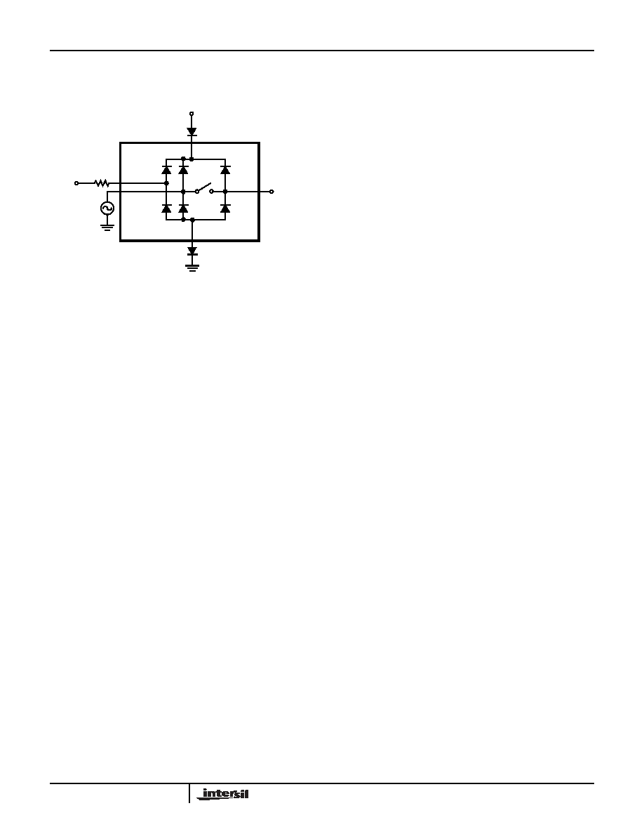
FIGURE 8. OVERVOLTAGE PROTECTION
V-
VCOM
VNO or NC
OPTIONAL PROTECTION
V+
INX
DIODE
OPTIONAL PROTECTION
DIODE
OPTIONAL
PROTECTION
RESISTOR
ISL8394
相关PDF资料 |
PDF描述 |
|---|---|
| ISL84053IB-T | IC MUX/DEMUX TRIPLE 2X1 16SOIC |
| ISL84467IVZ | IC SWITCH QUAD SPDT 16TSSOP |
| ISL84515IB-T | IC SWITCH SPST 8SOIC |
| ISL84517IB-T | IC SWITCH SPST 8SOIC |
| ISL84523IV-T | IC SWITCH QUAD SPST 16TSSOP |
相关代理商/技术参数 |
参数描述 |
|---|---|
| ISL8394IBZ | 功能描述:IC SWITCH QUAD SPDT 20SOIC RoHS:是 类别:集成电路 (IC) >> 接口 - 模拟开关,多路复用器,多路分解器 系列:- 产品培训模块:Lead (SnPb) Finish for COTS Obsolescence Mitigation Program 标准包装:36 系列:- 功能:多路复用器 电路:2 x 4:1 导通状态电阻:75 欧姆 电压电源:单/双电源 电压 - 电源,单路/双路(±):2 V ~ 12 V,±2 V ~ 6 V 电流 - 电源:- 工作温度:0°C ~ 70°C 安装类型:表面贴装 封装/外壳:20-SOIC(0.295",7.50mm 宽) 供应商设备封装:20-SOIC W 包装:管件 |
| ISL8394IBZ-T | 功能描述:IC SWITCH QUAD SPDT 20SOIC RoHS:是 类别:集成电路 (IC) >> 接口 - 模拟开关,多路复用器,多路分解器 系列:- 产品培训模块:Lead (SnPb) Finish for COTS Obsolescence Mitigation Program 标准包装:36 系列:- 功能:多路复用器 电路:2 x 4:1 导通状态电阻:75 欧姆 电压电源:单/双电源 电压 - 电源,单路/双路(±):2 V ~ 12 V,±2 V ~ 6 V 电流 - 电源:- 工作温度:0°C ~ 70°C 安装类型:表面贴装 封装/外壳:20-SOIC(0.295",7.50mm 宽) 供应商设备封装:20-SOIC W 包装:管件 |
| ISL84051 | 制造商:INTERSIL 制造商全称:Intersil Corporation 功能描述:Low Voltage, Single and Dual Supply, 8 to 1 Multiplexer, Dual 4 to 1 Multiplexer and a Triple SPDT Analog Switch |
| ISL84051_07 | 制造商:INTERSIL 制造商全称:Intersil Corporation 功能描述:Low Voltage, Single and Dual Supply, 8 to 1 Multiplexer, Dual 4 to 1 Multiplexer and a Triple SPDT Analog Switch |
| ISL84051_0710 | 制造商:INTERSIL 制造商全称:Intersil Corporation 功能描述:Low Voltage, Single and Dual Supply, 8 to 1 Multiplexer, Dual 4 to 1 Multiplexer and a Triple SPDT Analog Switch |
发布紧急采购,3分钟左右您将得到回复。