- 您现在的位置:买卖IC网 > PDF目录11170 > ISL8394IBZ-T (Intersil)IC SWITCH QUAD SPDT 20SOIC PDF资料下载
参数资料
| 型号: | ISL8394IBZ-T |
| 厂商: | Intersil |
| 文件页数: | 5/11页 |
| 文件大小: | 0K |
| 描述: | IC SWITCH QUAD SPDT 20SOIC |
| 标准包装: | 1,000 |
| 功能: | 开关 |
| 电路: | 4 x SPDT |
| 导通状态电阻: | 35 欧姆 |
| 电压电源: | 单/双电源 |
| 电压 - 电源,单路/双路(±): | 2 V ~ 12 V,±2 V ~ 6 V |
| 电流 - 电源: | 10nA |
| 工作温度: | -40°C ~ 85°C |
| 安装类型: | 表面贴装 |
| 封装/外壳: | 20-SOIC(0.295",7.50mm 宽) |
| 供应商设备封装: | 20-SOIC W |
| 包装: | 带卷 (TR) |
3
FN6038.3
March 13, 2006
Absolute Maximum Ratings
Thermal Information
V+ to V- . . . . . . . . . . . . . . . . . . . . . . . . . . . . . . . . . . . . . . -0.3 to15V
V+ to GND . . . . . . . . . . . . . . . . . . . . . . . . . . . . . . . . . . . . -0.3 to15V
V- to GND. . . . . . . . . . . . . . . . . . . . . . . . . . . . . . . . . . . . -15 to 0.3V
All Other Pins (Note 2) . . . . . . . . . . . . . ((V-) - 0.3V) to ((V+) + 0.3V)
Continuous Current (Any Terminal) . . . . . . . . . . . . . . . . . . . . . 30mA
Peak Current, IN, NO, NC, or COM
(Pulsed 1ms, 10% Duty Cycle, Max) . . . . . . . . . . . . . . . . . 100mA
ESD Rating (Per MIL-STD-883 Method 3015). . . . . . . . . . . . . .>2kV
Operating Conditions
Temperature Range
ISL8394IX . . . . . . . . . . . . . . . . . . . . . . . . . . . . . . . . . -40°C to 85°C
Thermal Resistance (Typical, Note 3)
θJA (°C/W)
20 Ld SOIC Package . . . . . . . . . . . . . . . . . . . . . . . .
95
Maximum Junction Temperature (Plastic Package). . . . . . . . 150°C
Moisture Sensitivity (See Technical Brief TB363)
SOIC Package . . . . . . . . . . . . . . . . . . . . . . . . . . . . . . . . . . Level 1
Maximum Storage Temperature Range . . . . . . . . . . . . . -65°C to 150°C
Maximum Lead Temperature (Soldering 10s) . . . . . . . . . . . . 300°C
(Lead Tips Only)
CAUTION: Stresses above those listed in “Absolute Maximum Ratings” may cause permanent damage to the device. This is a stress only rating and operation of the
device at these or any other conditions above those indicated in the operational sections of this specification is not implied.
NOTES:
2. Signals on NC, NO, COM, or IN exceeding V+ or V- are clamped by internal diodes. Limit forward diode current to maximum current ratings.
3.
θJA is measured with the component mounted on a low effective thermal conductivity test board in free air. See Tech Brief TB379 for details.
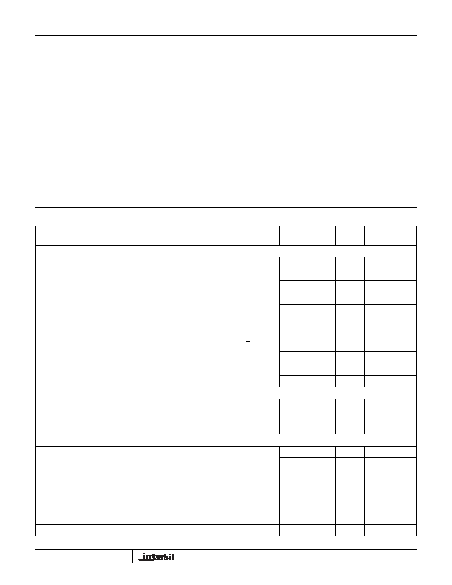
Electrical Specifications: ±5V Supply Test Conditions: VSUPPLY = ±4.5V to ±5.5V, GND = 0V, VINH = 2.4V, VINL = 0.8V (Note 4),
Unless Otherwise Specified
PARAMETER
TEST CONDITIONS
TEMP
(°C)
(NOTE 5)
MIN
TYP
(NOTE 5)
MAX
UNITS
ANALOG SWITCH CHARACTERISTICS
Analog Signal Range, VANALOG
Full
V-
-
V+
V
ON Resistance, RON
VS = ±4.5V, ICOM = 10mA, VNO or VNC = ±3.5V,
(See Figure 5)
25
-
17
35
Full
-
45
RON Matching Between Channels,
RON
VS = ±5V, ICOM = 10mA, VNO or VNC = ±3V
25
-
0.5
2
Full
-
4
RON Flatness, RFLAT(ON)
VS = ±5V, ICOM = 10mA, VNO or VNC = ±3V, 0V,
(Note 7)
25
-
4
Full
-
6
NO or NC OFF Leakage Current,
INO(OFF) or INC(OFF)
VS = ±5.5V, VCOM = ±4.5V, VNO or VNC = +4.5V,
(Note 6)
25
-0.2
-
0.2
nA
Full
-2.5
-
2.5
nA
COM ON Leakage Current,
ICOM(ON)
VS = ±5.5V, VCOM = VNO or VNC = ±4.5V, (Note 6)
25
-0.4
-
0.4
nA
Full
-5
-
5
nA
DIGITAL INPUT CHARACTERISTICS
Input Voltage High, VINH
Full
2.4
-
V
Input Voltage Low, VINL
Full
-
0.8
V
Input Current, IINH, IINL
VS = ±5.5V, VIN = 0V or V+
Full
-1
1
A
DYNAMIC CHARACTERISTICS
Turn-ON Time, tON
VS = ±4.5V, VNO or VNC = ±3V, RL = 300, CL = 35pF,
VIN = 0 to 3V, (See Figure 1)
25
-
50
130
ns
Full
-
175
ns
Turn-OFF Time, tOFF
VS = ±4.5V, VNO or VNC = ±3V, RL = 300, CL = 35pF,
VIN = 0 to 3V, (See Figure 1)
25
-
30
75
ns
Full
-
100
ns
Break-Before-Make Time Delay, tD
VS = ±5.5V, VNO or VNC = 3V, RL = 300, CL = 35pF,
VIN = 0 to 3V, (See Figure 3)
25
2
10
-
ns
Charge Injection, Q
CL = 1.0nF, VG = 0V, RG = 0, (See Figure 2)
25
-
5
10
pC
NO OFF Capacitance, COFF
f = 1MHz, VNO or VNC = VCOM = 0V, (See Figure 7)
25
-
12
-
pF
ISL8394
相关PDF资料 |
PDF描述 |
|---|---|
| C8051F818-GU | IC MCU 8BIT 8KB FLASH 24QSOP |
| C8051F809-GS | IC MCU 8BIT 16KB FLASH 16SOIC |
| HA4314BCPZ | IC VIDEO CROSSPOINT SWITCH 14DIP |
| P80C32SBBB,557 | IC 80C51 MCU 256 ROMLESS 44-QFP |
| P80C31SFAA,512 | IC 80C51 MCU 8BIT ROMLESS 44PLCC |
相关代理商/技术参数 |
参数描述 |
|---|---|
| ISL84051 | 制造商:INTERSIL 制造商全称:Intersil Corporation 功能描述:Low Voltage, Single and Dual Supply, 8 to 1 Multiplexer, Dual 4 to 1 Multiplexer and a Triple SPDT Analog Switch |
| ISL84051_07 | 制造商:INTERSIL 制造商全称:Intersil Corporation 功能描述:Low Voltage, Single and Dual Supply, 8 to 1 Multiplexer, Dual 4 to 1 Multiplexer and a Triple SPDT Analog Switch |
| ISL84051_0710 | 制造商:INTERSIL 制造商全称:Intersil Corporation 功能描述:Low Voltage, Single and Dual Supply, 8 to 1 Multiplexer, Dual 4 to 1 Multiplexer and a Triple SPDT Analog Switch |
| ISL84051IA | 功能描述:IC MUX/DEMUX 8X1 16QSOP RoHS:否 类别:集成电路 (IC) >> 接口 - 模拟开关,多路复用器,多路分解器 系列:- 标准包装:48 系列:- 功能:开关 电路:4 x SPST - NO 导通状态电阻:100 欧姆 电压电源:单/双电源 电压 - 电源,单路/双路(±):2 V ~ 12 V,±2 V ~ 6 V 电流 - 电源:50nA 工作温度:-40°C ~ 85°C 安装类型:表面贴装 封装/外壳:16-SOIC(0.154",3.90mm 宽) 供应商设备封装:16-SOIC 包装:管件 |
| ISL84051IA-T | 功能描述:IC MUX/DEMUX 8X1 16QSOP RoHS:否 类别:集成电路 (IC) >> 接口 - 模拟开关,多路复用器,多路分解器 系列:- 标准包装:48 系列:- 功能:开关 电路:4 x SPST - NO 导通状态电阻:100 欧姆 电压电源:单/双电源 电压 - 电源,单路/双路(±):2 V ~ 12 V,±2 V ~ 6 V 电流 - 电源:50nA 工作温度:-40°C ~ 85°C 安装类型:表面贴装 封装/外壳:16-SOIC(0.154",3.90mm 宽) 供应商设备封装:16-SOIC 包装:管件 |
发布紧急采购,3分钟左右您将得到回复。