- 您现在的位置:买卖IC网 > PDF目录11154 > ISL84515IH-T (Intersil)IC SWITCH SPST SOT23-5 PDF资料下载
参数资料
| 型号: | ISL84515IH-T |
| 厂商: | Intersil |
| 文件页数: | 5/11页 |
| 文件大小: | 0K |
| 描述: | IC SWITCH SPST SOT23-5 |
| 标准包装: | 1 |
| 功能: | 开关 |
| 电路: | 1 x SPST- NC |
| 导通状态电阻: | 20 欧姆 |
| 电压电源: | 单电源 |
| 电压 - 电源,单路/双路(±): | 2.4 V ~ 12 V |
| 电流 - 电源: | 1µA |
| 工作温度: | -40°C ~ 85°C |
| 安装类型: | 表面贴装 |
| 封装/外壳: | SC-74A,SOT-753 |
| 供应商设备封装: | SOT-23-5 |
| 包装: | 剪切带 (CT) |
| 产品目录页面: | 1247 (CN2011-ZH PDF) |
| 其它名称: | ISL84515IH-CT |
3
Absolute Maximum Ratings
Thermal Information
V+ to GND . . . . . . . . . . . . . . . . . . . . . . . . . . . . . . . . . . . . -0.3 to15V
Input Voltages
IN (Note 2) . . . . . . . . . . . . . . . . . . . . . . . . . . . . -0.3 to ((V+) + 0.3V)
NO, NC (Note 2) . . . . . . . . . . . . . . . . . . . . . . . -0.3 to ((V+) + 0.3V)
Output Voltages
COM (Note 2). . . . . . . . . . . . . . . . . . . . . . . . . . -0.3 to ((V+) + 0.3V)
Continuous Current (Any Terminal) . . . . . . . . . . . . . . . . . . . . . 20mA
Peak Current NO, NC, or COM
(Pulsed 1ms, 10% Duty Cycle, Max) . . . . . . . . . . . . . . . . . . . . 30mA
ESD Rating (Per MIL-STD-883 Method 3015). . . . . . . . . . . . . >2kV
Operating Conditions
Temperature Range
ISL8451XIX . . . . . . . . . . . . . . . . . . . . . . . . . . . . . . . . -40oC to 85oC
Thermal Resistance (Typical, Note 3)
θJA (oC/W)
5 Ld SOT-23 Package . . . . . . . . . . . . . . . . . . . . . . .
225
8 Ld SOIC Package . . . . . . . . . . . . . . . . . . . . . . . . .
170
Maximum Junction Temperature (Plastic Package) . . . . . . . . 150oC
Moisture Sensitivity (See Technical Brief TB363)
All Packages. . . . . . . . . . . . . . . . . . . . . . . . . . . . . . . . . . . . Level 1
Maximum Storage Temperature Range . . . . . . . . . . . . -65oC to 150oC
Maximum Lead Temperature (Soldering 10s) . . . . . . . . . . . . 300oC
(Lead Tips Only)
CAUTION: Stresses above those listed in “Absolute Maximum Ratings” may cause permanent damage to the device. This is a stress only rating and operation of the
device at these or any other conditions above those indicated in the operational sections of this specification is not implied.
NOTES:
2. Signals on NO, NC, COM, or IN exceeding V+ or GND are clamped by internal diodes. Limit forward diode current to maximum current ratings.
3.
θJA is measured with the component mounted on a low effective thermal conductivity test board in free air. See Tech Brief TB379 for details.
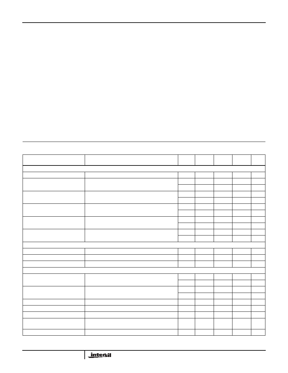
Electrical Specifications
Unless Otherwise Specified
PARAMETER
TEST CONDITIONS
TEMP
(oC)
(NOTE 5)
MIN
TYP
(NOTE 5)
MAX
UNITS
ANALOG SWITCH CHARACTERISTICS
Analog Signal Range, VANALOG
Full
0
-
V+
V
ON Resistance, RON
V+ = 4.5V, ICOM = 1.0mA, VCOM = 3.5V,
(See Figure 4)
25
-
20
Full
-
25
RON Flatness, RFLAT(ON)
V+ = 4.5V, ICOM = 1.0mA, VCOM = 1V, 2V, 3V
25
-
3
Full
-
5
NO or NC OFF Leakage Current,
INO(OFF) or INC(OFF)
V+ = 5.5V, VCOM = 1V, 4.5V, VNO or VNC = 4.5V, 1V,
(Note 6)
25
-1
0.01
1
nA
Full
-20
-
20
nA
COM OFF Leakage Current,
ICOM(OFF)
V+ = 5.5V, VCOM = 4.5V, 1V, VNO or VNC = 1V, 4.5V,
(Note 6)
25
-1
0.01
1
nA
Full
-20
-
20
nA
COM ON Leakage Current,
ICOM(ON)
V
+ = 5.5V, VCOM = 1V, 4.5V, or VNO or VNC = 1V,
4.5V, (Note 6)
25
-2
0.01
2
nA
Full
-40
-
40
nA
DIGITAL INPUT CHARACTERISTICS
Input Voltage High, VINH
Full
2.4
-
V+
V
Input Voltage Low, VINL
Full
0
-
0.8
V
Input Current, IINH, IINL
V+ = 5.5V, VIN = 0V or V+
Full
-1
-
1
A
DYNAMIC CHARACTERISTICS
Turn-ON Time, tON
VNO or VNC = 3V, RL = 300, CL = 35pF,
25
-
150
ns
Full
-
240
ns
Turn-OFF Time, tOFF
VNO or VNC = 3V, RL = 300, CL = 35pF,
25
-
100
ns
Full
-
150
ns
Charge Injection, Q
25
-
2
10
pC
OFF Isolation
25
-
>90
-
dB
25
-
14
-
pF
COM OFF Capacitance,
CCOM(OFF)
25
-
14
-
pF
COM ON Capacitance, CCOM(ON)
25
-
30
-
pF
ISL84514, ISL84515
相关PDF资料 |
PDF描述 |
|---|---|
| VE-211-IY-F2 | CONVERTER MOD DC/DC 12V 50W |
| MAX4617ESE+T | IC MULTIPLEXER 8X1 16SOIC |
| MAX4618ESE+T | IC MULTIPLEXER DUAL 4X1 16SOIC |
| VI-B63-IW-F2 | CONVERTER MOD DC/DC 24V 100W |
| VI-B63-IW-F1 | CONVERTER MOD DC/DC 24V 100W |
相关代理商/技术参数 |
参数描述 |
|---|---|
| ISL84515IHZ-T | 功能描述:IC SWITCH SPST SOT23-5 RoHS:是 类别:集成电路 (IC) >> 接口 - 模拟开关,多路复用器,多路分解器 系列:- 产品培训模块:Lead (SnPb) Finish for COTS Obsolescence Mitigation Program 标准包装:36 系列:- 功能:多路复用器 电路:2 x 4:1 导通状态电阻:75 欧姆 电压电源:单/双电源 电压 - 电源,单路/双路(±):2 V ~ 12 V,±2 V ~ 6 V 电流 - 电源:- 工作温度:0°C ~ 70°C 安装类型:表面贴装 封装/外壳:20-SOIC(0.295",7.50mm 宽) 供应商设备封装:20-SOIC W 包装:管件 |
| ISL84516 | 制造商:INTERSIL 制造商全称:Intersil Corporation 功能描述:Low-Voltage, Dual Supply, SPST, Analog Switches |
| ISL84516_05 | 制造商:INTERSIL 制造商全称:Intersil Corporation 功能描述:Low-Voltage, Dual Supply, SPST, Analog Switches |
| ISL84516IB | 功能描述:IC SWITCH SPST 8SOIC RoHS:否 类别:集成电路 (IC) >> 接口 - 模拟开关,多路复用器,多路分解器 系列:- 标准包装:48 系列:- 功能:开关 电路:4 x SPST - NO 导通状态电阻:100 欧姆 电压电源:单/双电源 电压 - 电源,单路/双路(±):2 V ~ 12 V,±2 V ~ 6 V 电流 - 电源:50nA 工作温度:-40°C ~ 85°C 安装类型:表面贴装 封装/外壳:16-SOIC(0.154",3.90mm 宽) 供应商设备封装:16-SOIC 包装:管件 |
| ISL84516IB-T | 功能描述:IC SWITCH SPST 8SOIC RoHS:否 类别:集成电路 (IC) >> 接口 - 模拟开关,多路复用器,多路分解器 系列:- 标准包装:48 系列:- 功能:开关 电路:4 x SPST - NO 导通状态电阻:100 欧姆 电压电源:单/双电源 电压 - 电源,单路/双路(±):2 V ~ 12 V,±2 V ~ 6 V 电流 - 电源:50nA 工作温度:-40°C ~ 85°C 安装类型:表面贴装 封装/外壳:16-SOIC(0.154",3.90mm 宽) 供应商设备封装:16-SOIC 包装:管件 |
发布紧急采购,3分钟左右您将得到回复。