- 您现在的位置:买卖IC网 > PDF目录11174 > ISL84684IUZ (Intersil)IC SWITCH DUAL SPDT 10MSOP PDF资料下载
参数资料
| 型号: | ISL84684IUZ |
| 厂商: | Intersil |
| 文件页数: | 11/13页 |
| 文件大小: | 0K |
| 描述: | IC SWITCH DUAL SPDT 10MSOP |
| 标准包装: | 980 |
| 功能: | 开关 |
| 电路: | 2 x SPDT |
| 导通状态电阻: | 500 毫欧 |
| 电压电源: | 单电源 |
| 电压 - 电源,单路/双路(±): | 1.8 V ~ 4.5 V |
| 电流 - 电源: | 40nA |
| 工作温度: | -40°C ~ 85°C |
| 安装类型: | 表面贴装 |
| 封装/外壳: | 10-TFSOP,10-MSOP(0.118",3.00mm 宽) |
| 供应商设备封装: | 10-MSOP |
| 包装: | 管件 |
7
FN6088.5
July 31, 2007
During an overvoltage transient event, such as occurs during
system level IEC 61000 ESD testing, substrate currents can
be generated in the IC that can trigger parasitic SCR
structures to turn ON, creating a low impedance path from
the V+ power supply to ground. This will result in a
significant amount of current flow in the IC which can
potentially create a latch-up state or permanently damage
the IC. The external V+ resistor limits the current during this
over-stress situation and has been found to prevent latch-up
or destructive damage for many overvoltage transient
events.
Under normal operation, the sub-microamp IDD current of
the IC produces an insignificant voltage drop across the
100
Ω series resistor resulting in no impact to switch
operation or performance.
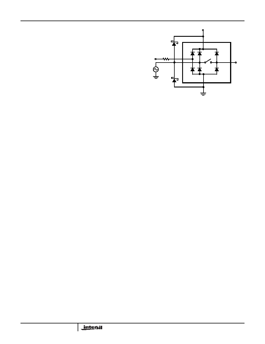
Supply Sequencing and Overvoltage Protection
With any CMOS device, proper power supply sequencing is
required to protect the device from excessive input currents
which might permanently damage the IC. All I/O pins contain
ESD protection diodes from the pin to V+ and to GND (see
Figure 9). To prevent forward biasing these diodes, V+ must
be applied before any input signals and the input signal
voltages must remain between V+ and GND.
If these conditions cannot be guaranteed, then precautions
must be implemented to prohibit the current and voltage at
the logic pin and signal pins from exceeding the maximum
ratings of the switch. The following two methods can be used
to provide additional protection to limit the current in the
event that the voltage at a signal pin or logic pin goes below
ground or above the V+ rail.
Logic inputs can easily be protected by adding a 1k
Ω
resistor in series with the input (see Figure 9). The resistor
limits the input current below the threshold that produces
permanent damage and the sub-microamp input current
produces an insignificant voltage drop during normal
operation.
This method is not acceptable for the signal path inputs.
Adding a series resistor to the switch input defeats the
purpose of using a low rON switch. Connecting Schottky
diodes to the signal pins as shown in Figure 9 will shunt the
fault current to the supply or to ground thereby protecting the
switch. These Schottky diodes must be sized to handle the
expected fault current.
.
Power-Supply Considerations
The ISL84684 construction is typical of most single supply
CMOS analog switches, in that they have two supply pins:
V+ and GND. V+ and GND drive the internal CMOS
switches and set their analog voltage limits. Unlike switches
with a 4V maximum supply voltage, the ISL84684 5.5V
maximum supply voltage provides plenty of room for the
10% tolerance of 4.3V supplies, as well as room for
overshoot and noise spikes.
The minimum recommended supply voltage is 1.65V. It is
important to note that the input signal range, switching times,
and ON-resistance degrade at lower supply voltages. Refer
to the “Electrical Specification” tables on page 2 and “Typical
Performance Curves” on page 9 for details.
V+ and GND also power the internal logic and level shiftiers.
The level shiftiers convert the input logic levels to switched
V+ and GND signals to drive the analog switch gate
terminals.
This family of switches cannot be operated with bipolar
supplies because the input switching point becomes
negative in this configuration.
Logic-Level Thresholds
This switch family is 1.8V CMOS compatible (0.5V and 1.4V)
over a supply range of 2.7V to 4.5V (see Figure 18). At 2.7V,
the VIL level is about 0.53V. This is still above the 1.8V
CMOS guaranteed low output minimum level of 0.5V, but
noise margin is reduced.
The digital input stages draw supply current whenever the
digital input voltage is not at one of the supply rails. Driving
the digital input signals from GND to V+ with a fast transition
time minimizes power dissipation.
GND
VCOM
VNX
V+
INX
OPTIONAL
PROTECTION
RESISTOR
OPTIONAL
SCHOTTKY
DIODE
OPTIONAL
SCHOTTKY
DIODE
FIGURE 9. OVERVOLTAGE PROTECTION
ISL84684
相关PDF资料 |
PDF描述 |
|---|---|
| ISL8484IUZ | IC SWITCH DUAL SPDT 10MSOP |
| ISL43L120IRZ-T | IC SWITCH DUAL SPST 8TDFN |
| VI-B22-IW | CONVERTER MOD DC/DC 15V 100W |
| VE-JNM-IW | CONVERTER MOD DC/DC 10V 100W |
| PI3L110LE | IC ETHERNET SWITCH QUAD 16TSSOP |
相关代理商/技术参数 |
参数描述 |
|---|---|
| ISL84684IUZ-T | 功能描述:IC SWITCH DUAL SPDT 10MSOP RoHS:是 类别:集成电路 (IC) >> 接口 - 模拟开关,多路复用器,多路分解器 系列:- 产品培训模块:Lead (SnPb) Finish for COTS Obsolescence Mitigation Program 标准包装:36 系列:- 功能:多路复用器 电路:2 x 4:1 导通状态电阻:75 欧姆 电压电源:单/双电源 电压 - 电源,单路/双路(±):2 V ~ 12 V,±2 V ~ 6 V 电流 - 电源:- 工作温度:0°C ~ 70°C 安装类型:表面贴装 封装/外壳:20-SOIC(0.295",7.50mm 宽) 供应商设备封装:20-SOIC W 包装:管件 |
| ISL84714 | 制造商:INTERSIL 制造商全称:Intersil Corporation 功能描述:Ultra Low ON-Resistance, Low Voltage, Single Supply, SPDT Analog Switch |
| ISL84714_0411 | 制造商:INTERSIL 制造商全称:Intersil Corporation 功能描述:Ultra Low ON-Resistance, Low Voltage, Single Supply, SPDT Analog Switch |
| ISL84714IH-T | 功能描述:IC SWITCH SPDT SC70-6 RoHS:否 类别:集成电路 (IC) >> 接口 - 模拟开关,多路复用器,多路分解器 系列:- 标准包装:48 系列:- 功能:开关 电路:4 x SPST - NO 导通状态电阻:100 欧姆 电压电源:单/双电源 电压 - 电源,单路/双路(±):2 V ~ 12 V,±2 V ~ 6 V 电流 - 电源:50nA 工作温度:-40°C ~ 85°C 安装类型:表面贴装 封装/外壳:16-SOIC(0.154",3.90mm 宽) 供应商设备封装:16-SOIC 包装:管件 |
| ISL84714IHZ-T | 功能描述:IC SWITCH SPDT SC70-6 RoHS:是 类别:集成电路 (IC) >> 接口 - 模拟开关,多路复用器,多路分解器 系列:- 标准包装:2,500 系列:- 功能:视频交叉点开关 电路:1 x 8:6 导通状态电阻:- 电压电源:单电源 电压 - 电源,单路/双路(±):3.135 V ~ 5.25 V 电流 - 电源:55mA 工作温度:-40°C ~ 85°C 安装类型:表面贴装 封装/外壳:24-TSSOP(0.173",4.40mm 宽) 供应商设备封装:24-TSSOP 包装:带卷 (TR) 产品目录页面:1214 (CN2011-ZH PDF) 其它名称:FMS6502MTC24XTR |
发布紧急采购,3分钟左右您将得到回复。