- 您现在的位置:买卖IC网 > PDF目录11411 > ISL84716IH-T (Intersil)IC SWITCH SPST SC70-5 PDF资料下载
参数资料
| 型号: | ISL84716IH-T |
| 厂商: | Intersil |
| 文件页数: | 7/10页 |
| 文件大小: | 0K |
| 描述: | IC SWITCH SPST SC70-5 |
| 标准包装: | 1 |
| 功能: | 开关 |
| 电路: | 1 x SPST- NC |
| 导通状态电阻: | 400 毫欧 |
| 电压电源: | 单电源 |
| 电压 - 电源,单路/双路(±): | 1.65 V ~ 3.6 V |
| 电流 - 电源: | 18nA |
| 工作温度: | -40°C ~ 85°C |
| 安装类型: | 表面贴装 |
| 封装/外壳: | 6-TSSOP(5 引线),SC-88A,SOT-353 |
| 供应商设备封装: | SC-70-5 |
| 包装: | 标准包装 |
| 其它名称: | ISL84716IH-DKR ISL84716IH-DKR-ND ISL84716IHDKR |
ISL84715, ISL84716
6
FN6087.3
February 23, 2012
Detailed Description
The ISL84715 and ISL84716 are bidirectional, single pole/single
throw (SPST) analog switches. They offer precise switching
capability from a single 1.65V to 3.6V supply with ultra low
on-resistance and high speed operation. With a single supply of 3V
the typical on-resistance is only 0.26, with a typical turn-on and
turn-off time of: tON =9ns, tOFF = 5ns. The devices are especially
well suited for portable battery powered equipment due to its low
operating supply voltage (1.65V), low power consumption (1.05W),
low leakage currents (35nA max), and the tiny SC70 packaging.
The ISL84715 is a normally open (NO) SPST analog switch. The
ISL84716 is a normally closed (NC) SPST analog switch.
Supply Sequencing and Overvoltage
Protection
With any CMOS device, proper power supply sequencing is
required to protect the device from excessive input currents
which might permanently damage the IC. All I/O pins contain
ESD protection diodes from the pin to V+ and to GND (see
Figure 6). To prevent forward biasing these diodes, V+ must be
applied before any input signals, and the input signal voltages
must remain between V+ and GND.
If these conditions cannot be guaranteed, then precautions must be
implemented to prohibit the current and voltage at the logic pin and
signal pins from exceeding the maximum ratings of the switch. The
following two methods can be used to provided additional protection
to limit the current in the event that the voltage at a signal pin or
logic pin goes below ground or above the V+ rail.
Logic inputs can be protected by adding a 1k resistor in series
with the logic input (see Figure 6). The resistor limits the input
current below the threshold that produces permanent damage,
and the sub-microamp input current produces an insignificant
voltage drop during normal operation.
This method is not acceptable for the signal path inputs. Adding
a series resistor to the switch input defeats the purpose of using
a low rON switch. Connecting Schottky diodes to the signal pins
(as shown in Figure 6) will shunt the fault current to the supply or
to ground thereby protecting the switch. These Schottky diodes
must be sized to handle the expected fault current.
Power-Supply Considerations
The ISL8471X construction is typical of most single supply CMOS
analog switches in that they have two supply pins: V+ and GND.
V+ and GND drive the internal CMOS switches and set their
analog voltage limits. Unlike switches with a 4V maximum supply
voltage, the ISL84714 4.8V maximum supply voltage provides
plenty of room for the 10% tolerance of 3.6V supplies, as well as
room for overshoot and noise spikes.
The minimum recommended supply voltage is 3.6V but the part
will operate with a supply below 1.5V. It is important to note that
the input signal range, switching times, and on-resistance
degrade at lower supply voltages. Refer to the electrical
specification tables and Typical Performance curves for details.
V+ and GND also power the internal logic and level shiftier. The
level shiftier converts the input logic levels to switched V+ and
GND signals to drive the analog switch gate terminals.
This family of switches cannot be operated with bipolar supplies,
because the input switching point becomes negative in this
configuration.
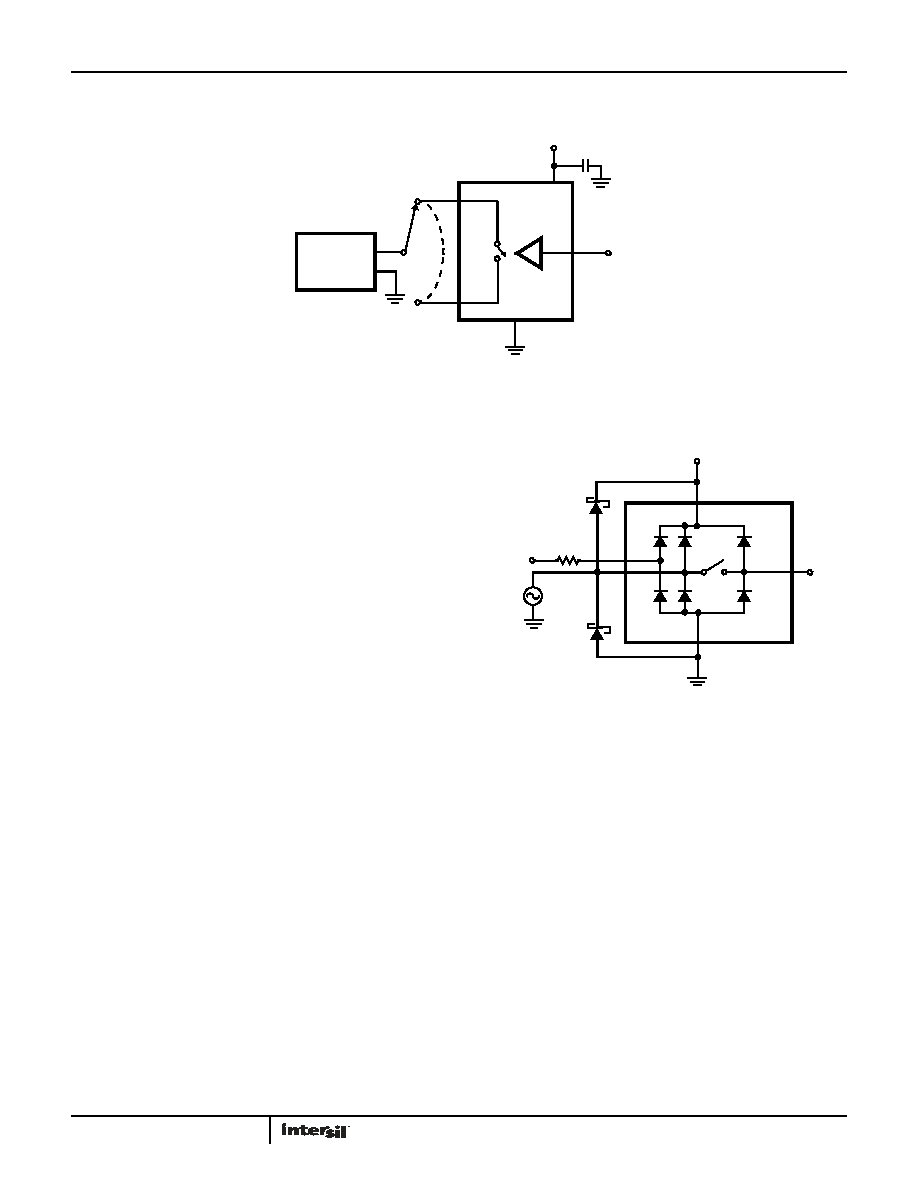
FIGURE 5. CAPACITANCE TEST CIRCUIT
Test Circuits and Waveforms (Continued)
V+
C
GND
NO or NC
COM
IN
IMPEDANCE
ANALYZER
0V or V+
FIGURE 6. OVERVOLTAGE PROTECTION
GND
VCOM
VNX
V+
INX
OPTIONAL
PROTECTION
RESISTOR
OPTIONAL
SCHOTTKY
DIODE
OPTIONAL
SCHOTTKY
DIODE
相关PDF资料 |
PDF描述 |
|---|---|
| PIC18F67J60T-I/PT | IC PIC MCU FLASH 64KX16 64TQFP |
| VI-2NP-CV-F3 | CONVERTER MOD DC/DC 13.8V 150W |
| GRM219R71E824KA88D | CAP CER 0.82UF 25V 10% X7R 0805 |
| VI-2NP-CV-F1 | CONVERTER MOD DC/DC 13.8V 150W |
| GRM31MR72A224KA01L | CAP CER 0.22UF 100V 10% X7R 1206 |
相关代理商/技术参数 |
参数描述 |
|---|---|
| ISL84716IHZ-T | 功能描述:IC SWITCH SPST SC70-5 RoHS:是 类别:集成电路 (IC) >> 接口 - 模拟开关,多路复用器,多路分解器 系列:- 标准包装:1 系列:- 功能:开关 电路:2 x SPST - NC/NO 导通状态电阻:8 欧姆 电压电源:单电源 电压 - 电源,单路/双路(±):2.3 V ~ 4.3 V 电流 - 电源:1µA 工作温度:-40°C ~ 85°C 安装类型:表面贴装 封装/外壳:8-UFQFN 供应商设备封装:8-迷你型QFN(1.4x1.4) 包装:剪切带 (CT) 其它名称:DG2738DN-T1-E4CT |
| ISL84762 | 制造商:INTERSIL 制造商全称:Intersil Corporation 功能描述:Ultra Low ON-Resistance, Low Voltage, Single Supply, Dual SPDT Analog Switch |
| ISL84762IR | 功能描述:IC SWITCH DUAL SPDT 10TDFN RoHS:否 类别:集成电路 (IC) >> 接口 - 模拟开关,多路复用器,多路分解器 系列:- 产品培训模块:Obsolescence Mitigation Program 标准包装:2,500 系列:- 功能:- 电路:2 x SPST 导通状态电阻:20 欧姆 电压电源:单电源 电压 - 电源,单路/双路(±):3 V ~ 5.5 V 电流 - 电源:4.1mA 工作温度:-40°C ~ 85°C 安装类型:表面贴装 封装/外壳:10-WFDFN 裸露焊盘 供应商设备封装:10-TDFN-EP(3x3) 包装:带卷 (TR) |
| ISL84762IR-T | 功能描述:IC SWITCH DUAL SPDT 10TDFN RoHS:否 类别:集成电路 (IC) >> 接口 - 模拟开关,多路复用器,多路分解器 系列:- 产品培训模块:Obsolescence Mitigation Program 标准包装:2,500 系列:- 功能:- 电路:2 x SPST 导通状态电阻:20 欧姆 电压电源:单电源 电压 - 电源,单路/双路(±):3 V ~ 5.5 V 电流 - 电源:4.1mA 工作温度:-40°C ~ 85°C 安装类型:表面贴装 封装/外壳:10-WFDFN 裸露焊盘 供应商设备封装:10-TDFN-EP(3x3) 包装:带卷 (TR) |
| ISL84762IRZ | 功能描述:IC SWITCH DUAL SPDT 10TDFN RoHS:是 类别:集成电路 (IC) >> 接口 - 模拟开关,多路复用器,多路分解器 系列:- 产品培训模块:Lead (SnPb) Finish for COTS Obsolescence Mitigation Program 标准包装:36 系列:- 功能:多路复用器 电路:2 x 4:1 导通状态电阻:75 欧姆 电压电源:单/双电源 电压 - 电源,单路/双路(±):2 V ~ 12 V,±2 V ~ 6 V 电流 - 电源:- 工作温度:0°C ~ 70°C 安装类型:表面贴装 封装/外壳:20-SOIC(0.295",7.50mm 宽) 供应商设备封装:20-SOIC W 包装:管件 |
发布紧急采购,3分钟左右您将得到回复。