- 您现在的位置:买卖IC网 > PDF目录11172 > ISL8499IRTZ (Intersil)IC SWITCH QUAD SPDT 16TQFN PDF资料下载
参数资料
| 型号: | ISL8499IRTZ |
| 厂商: | Intersil |
| 文件页数: | 13/14页 |
| 文件大小: | 0K |
| 描述: | IC SWITCH QUAD SPDT 16TQFN |
| 标准包装: | 100 |
| 功能: | 开关 |
| 电路: | 4 x SPDT |
| 导通状态电阻: | 250 毫欧 |
| 电压电源: | 单电源 |
| 电压 - 电源,单路/双路(±): | 1.65 V ~ 4.5 V |
| 电流 - 电源: | 90nA |
| 工作温度: | -40°C ~ 85°C |
| 安装类型: | 表面贴装 |
| 封装/外壳: | 16-WFQFN 裸露焊盘 |
| 供应商设备封装: | 16-QFN-EP(3x3) |
| 包装: | 管件 |
8
FN6111.3
February 5, 2008
additional diodes limit the analog signal from 1V below V+ to
1V above GND. The low leakage current performance is
unaffected by this approach, but the switch signal range is
reduced and the resistance may increase, especially at low
supply voltages.
Power-Supply Considerations
The ISL8499 construction is typical of most single supply
CMOS analog switches, in that they have two supply pins:
V+ and GND. V+ and GND drive the internal CMOS
switches and set their analog voltage limits. Unlike switches
with a 4V maximum supply voltage, the ISL8499 4.7V
maximum supply voltage provides plenty of room for the
10% tolerance of 4.3V supplies, as well as room for
overshoot and noise spikes.
The minimum recommended supply voltage is 1.65V but will
operate with a supply voltage below 1.5V. It is important to
note that the input signal range, switching times, and
on-resistance degrade at lower supply voltages. Refer to the
“Electrical Specification” tables starting on page 3 and
“Typical Performance” curves starting on page 6 for details.
V+ and GND also power the internal logic and level shiftiers.
The level shiftiers convert the input logic levels to switched
V+ and GND signals to drive the analog switch gate
terminals.
This family of switches cannot be operated with bipolar
supplies, because the input switching point becomes
negative in this configuration.
Logic-Level Thresholds
This switch family is 1.8V CMOS compatible (0.5V and 1.4V)
over a supply range of 2.7V to 4.5V (see Figure 14). At 2.7V
the VIL level is about 0.52V. This is still above the 1.8V
CMOS guaranteed low output maximum level of 0.5V, but
noise margin is reduced.
The digital input stages draw supply current whenever the
digital input voltage is not at one of the supply rails. Driving
the digital input signals from GND to V+ with a fast transition
time minimizes power dissipation. The ISL8499 has been
designed to minimize the supply current whenever the digital
input voltage is not driven to the supply rails (0V to V+). For
example driving the device with 2.85V logic (0V to 2.85V)
while operating with a 4.2V supply the device draws only
6
μA of current (see Figure 21 for VIN = 2.85V).
High-Frequency Performance
In 50
Ω systems, the signal response is reasonably flat even
past 30MHz with a -3dB bandwidth of 104MHz (see
Figure 17). The frequency response is very consistent over a
wide V+ range, and for varying analog signal levels.
An OFF switch acts like a capacitor and passes higher
frequencies with less attenuation, resulting in signal
feedthrough from a switch’s input to its output. Off Isolation is
the resistance to this feedthrough, while Crosstalk indicates
the amount of feedthrough from one switch to another.
Figure 18 details the high Off Isolation and Crosstalk
rejection provided by this part. At 100kHz, Off Isolation is
about 68dB in 50
Ω systems, decreasing approximately 20dB
per decade as frequency increases. Higher load
impedances decrease Off Isolation and Crosstalk rejection
due to the voltage divider action of the switch OFF
impedance and the load impedance.
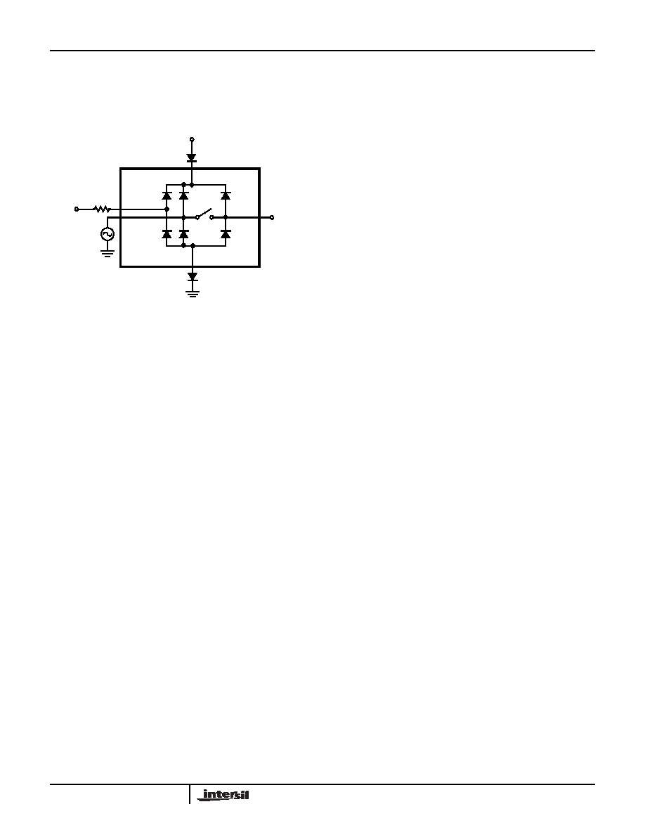
Leakage Considerations
Reverse ESD protection diodes are internally connected
between each analog-signal pin and both V+ and GND. One of
these diodes conducts if any analog signal exceeds V+ or
GND.
Virtually all the analog leakage current comes from the ESD
diodes to V+ or GND. Although the ESD diodes on a given
signal pin are identical and therefore fairly well balanced,
they are reverse biased differently. Each is biased by either
V+ or GND and the analog signal. This means their leakages
will vary as the signal varies. The difference in the two diode
leakages to the V+ and GND pins constitutes the analog-
signal-path leakage current. All analog leakage current flows
between each pin and one of the supply terminals, not to the
other switch terminal. This is why both sides of a given
switch can show leakage currents of the same or opposite
polarity. There is no connection between the analog signal
paths and V+ or GND.
FIGURE 8. OVERVOLTAGE PROTECTION
GND
VCOM
VNO or NC
OPTIONAL PROTECTION
V+
INX
DIODE
OPTIONAL PROTECTION
DIODE
OPTIONAL
PROTECTION
RESISTOR
ISL8499
相关PDF资料 |
PDF描述 |
|---|---|
| PI5L100QE | IC ETHERNET SWITCH QUAD 16QSOP |
| PI3L100QE | IC ETHERNET SWITCH QUAD 16QSOP |
| ISL43741IRZ | IC MUX/DEMUX DUAL 4X1 20QFN |
| ISL43231IRZ | IC SWITCH TRIPLE SPDT 20QFN |
| ISL8499IRZ-T | IC SWITCH QUAD SPDT 16QFN |
相关代理商/技术参数 |
参数描述 |
|---|---|
| ISL8499IRTZ-T | 功能描述:IC SWITCH QUAD SPDT 16TQFN RoHS:是 类别:集成电路 (IC) >> 接口 - 模拟开关,多路复用器,多路分解器 系列:- 产品培训模块:Lead (SnPb) Finish for COTS Obsolescence Mitigation Program 标准包装:36 系列:- 功能:多路复用器 电路:2 x 4:1 导通状态电阻:75 欧姆 电压电源:单/双电源 电压 - 电源,单路/双路(±):2 V ~ 12 V,±2 V ~ 6 V 电流 - 电源:- 工作温度:0°C ~ 70°C 安装类型:表面贴装 封装/外壳:20-SOIC(0.295",7.50mm 宽) 供应商设备封装:20-SOIC W 包装:管件 |
| ISL8499IRZ | 功能描述:IC SWITCH QUAD SPDT 16QFN RoHS:是 类别:集成电路 (IC) >> 接口 - 模拟开关,多路复用器,多路分解器 系列:- 标准包装:1 系列:- 功能:开关 电路:2 x SPST - NC/NO 导通状态电阻:8 欧姆 电压电源:单电源 电压 - 电源,单路/双路(±):2.3 V ~ 4.3 V 电流 - 电源:1µA 工作温度:-40°C ~ 85°C 安装类型:表面贴装 封装/外壳:8-UFQFN 供应商设备封装:8-迷你型QFN(1.4x1.4) 包装:剪切带 (CT) 其它名称:DG2738DN-T1-E4CT |
| ISL8499IRZ-T | 功能描述:IC SWITCH QUAD SPDT 16QFN RoHS:是 类别:集成电路 (IC) >> 接口 - 模拟开关,多路复用器,多路分解器 系列:- 产品培训模块:Lead (SnPb) Finish for COTS Obsolescence Mitigation Program 标准包装:36 系列:- 功能:多路复用器 电路:2 x 4:1 导通状态电阻:75 欧姆 电压电源:单/双电源 电压 - 电源,单路/双路(±):2 V ~ 12 V,±2 V ~ 6 V 电流 - 电源:- 工作温度:0°C ~ 70°C 安装类型:表面贴装 封装/外壳:20-SOIC(0.295",7.50mm 宽) 供应商设备封装:20-SOIC W 包装:管件 |
| ISL8499IV | 功能描述:IC SWITCH QUAD SPDT 16TSSOP RoHS:否 类别:集成电路 (IC) >> 接口 - 模拟开关,多路复用器,多路分解器 系列:- 产品培训模块:Obsolescence Mitigation Program 标准包装:2,500 系列:- 功能:- 电路:2 x SPST 导通状态电阻:20 欧姆 电压电源:单电源 电压 - 电源,单路/双路(±):3 V ~ 5.5 V 电流 - 电源:4.1mA 工作温度:-40°C ~ 85°C 安装类型:表面贴装 封装/外壳:10-WFDFN 裸露焊盘 供应商设备封装:10-TDFN-EP(3x3) 包装:带卷 (TR) |
| ISL8499IV-T | 功能描述:IC SWITCH QUAD SPDT 16TSSOP RoHS:否 类别:集成电路 (IC) >> 接口 - 模拟开关,多路复用器,多路分解器 系列:- 产品培训模块:Obsolescence Mitigation Program 标准包装:2,500 系列:- 功能:- 电路:2 x SPST 导通状态电阻:20 欧姆 电压电源:单电源 电压 - 电源,单路/双路(±):3 V ~ 5.5 V 电流 - 电源:4.1mA 工作温度:-40°C ~ 85°C 安装类型:表面贴装 封装/外壳:10-WFDFN 裸露焊盘 供应商设备封装:10-TDFN-EP(3x3) 包装:带卷 (TR) |
发布紧急采购,3分钟左右您将得到回复。