参数资料
| 型号: | ISL8563ECB-T |
| 厂商: | Intersil |
| 文件页数: | 8/9页 |
| 文件大小: | 0K |
| 描述: | XMITTER/RCVR RS562/232 18-SOIC |
| 标准包装: | 1,000 |
| 类型: | 收发器 |
| 驱动器/接收器数: | 2/2 |
| 规程: | RS232,RS562 |
| 电源电压: | 3 V ~ 5.5 V |
| 安装类型: | 表面贴装 |
| 封装/外壳: | 18-SOIC(0.295",7.50mm 宽) |
| 供应商设备封装: | 18-SOIC W |
| 包装: | 带卷 (TR) |
8
storage capacitor yields a test that is much more severe than
the HBM test. The extra ESD protection built into this
device’s RS-562/232 pins allows the design of equipment
meeting level 4 criteria without the need for additional board
level protection on the RS-562/232 port.
AIR-GAP DISCHARGE TEST METHOD
For this test method, a charged probe tip moves toward the
IC pin until the voltage arcs to it. The current waveform
delivered to the IC pin depends on approach speed,
humidity, temperature, etc., so it is difficult to obtain
repeatable results. The “E” device RS-562/232 pins
withstand
±15kV air-gap discharges.
CONTACT DISCHARGE TEST METHOD
During the contact discharge test, the probe contacts the
tested pin before the probe tip is energized, thereby
eliminating the variables associated with the air-gap
discharge. The result is a more repeatable and predictable
test, but equipment limits prevent testing devices at voltages
higher than
±8kV. All “E” family devices survive ±8kV contact
discharges on the RS-562/232 pins.
Die Characteristics
SUBSTRATE POTENTIAL (POWERED UP):
GND
TRANSISTOR COUNT:
338
PROCESS:
Si Gate CMOS
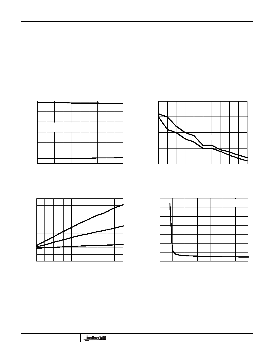
Typical Performance Curves VCC = 3.3V, TA = 25°C
FIGURE 10. TRANSMITTER OUTPUT VOLTAGE vs LOAD
CAPACITANCE
FIGURE 11. SLEW RATE vs LOAD CAPACITANCE
FIGURE 12. SUPPLY CURRENT vs LOAD CAPACITANCE
WHEN TRANSMITTING DATA
FIGURE 13. SUPPLY CURRENT vs SUPPLY VOLTAGE
-6
-4
-2
0
2
4
6
1000
2000
3000
4000
5000
0
LOAD CAPACITANCE (pF)
TRANSMITTER
OUT
P
UT
VOL
TAGE
(V)
1 TRANSMITTER AT 250kbps
VOUT+
VOUT -
1 TRANSMITTER AT 30kbps
LOAD CAPACITANCE (pF)
SLEW
RA
TE
(V
/s
)
0
1000
2000
3000
4000
5000
5
10
15
20
25
+SLEW
-SLEW
0
5
10
15
20
25
30
45
35
40
0
1000
2000
3000
4000
5000
LOAD CAPACITANCE (pF)
SUPPL
Y
CURR
E
N
T
(mA)
20kbps
250kbps
120kbps
SUP
P
LY
CURRENT
(m
A)
2.5
3.0
3.5
4.0
4.5
5.0
5.5
6.0
0
0.5
1.0
1.5
2.0
SUPPLY VOLTAGE (V)
2.5
3.0
3.5
NO LOAD
ALL OUTPUTS STATIC
ISL8563E
相关PDF资料 |
PDF描述 |
|---|---|
| ISL88694IH5-TK | IC SMBUS ACCELERATOR SOT23-5 |
| ISL90460WIH527-TK | IC XDCP 32-TAP 10KOHMS SOT23-5 |
| ISL90461WIH627-TK | IC XDCP 32-TAP 10KOHM SOT23-6 |
| ISL90462WIH627-TK | IC XDCP 32-TAP 10KOHM SOT23-6 |
| ISL90726UIE627Z | IC XDCP 128-TAP 50KOHM SC70-6 |
相关代理商/技术参数 |
参数描述 |
|---|---|
| ISL8563ECP | 制造商:Rochester Electronics LLC 功能描述:- Bulk 制造商:Intersil Corporation 功能描述: |
| ISL8563EIB | 制造商:Rochester Electronics LLC 功能描述:- Bulk 制造商:Intersil Corporation 功能描述: |
| ISL8563EIP | 制造商:Rochester Electronics LLC 功能描述:- Bulk |
| ISL8563IB | 制造商:Rochester Electronics LLC 功能描述:RS562 3V 2D/2R SHUTDOWN 18SOIC IND - Bulk |
| ISL8563IP | 制造商:Rochester Electronics LLC 功能描述:- Bulk |
发布紧急采购,3分钟左右您将得到回复。