- 您现在的位置:买卖IC网 > PDF目录20592 > ISL89160FRTAZ-T (Intersil)IC MOSFET DRIVER 2CH 6A 8TDFN PDF资料下载
参数资料
| 型号: | ISL89160FRTAZ-T |
| 厂商: | Intersil |
| 文件页数: | 9/14页 |
| 文件大小: | 0K |
| 描述: | IC MOSFET DRIVER 2CH 6A 8TDFN |
| 标准包装: | 6,000 |
| 配置: | 低端 |
| 输入类型: | 非反相 |
| 延迟时间: | 25ns |
| 电流 - 峰: | 6A |
| 配置数: | 2 |
| 输出数: | 2 |
| 电源电压: | 4.5 V ~ 16 V |
| 工作温度: | -40°C ~ 125°C |
| 安装类型: | 表面贴装 |
| 封装/外壳: | 8-WDFN 裸露焊盘 |
| 供应商设备封装: | 8-TDFN-EP(3x3) |
| 包装: | 带卷 (TR) |
�� �
�
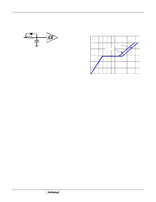
�ISL89160,� ISL89161,� ISL89162�
�In� Figure� 16,� R� del� and� C� del� delay� the� rising� edge� of� the� input�
�signal.� For� the� falling� edge� of� the� input� signal,� the� diode� shorts�
�out� the� resistor� resulting� in� a� minimal� falling� edge� delay.� If� the�
�diode� polarity� is� reversed,� the� falling� edge� is� delayed� and� the�
�rising� delay� is� minimal.�
�D�
�Power� Dissipation� of� the� Driver�
�The� power� dissipation� of� the� ISL89160,� ISL89161,� ISL89162� is�
�dominated� by� the� losses� associated� with� the� gate� charge� of� the�
�driven� bridge� FETs� and� the� switching� frequency.� The� internal� bias�
�current� also� contributes� to� the� total� dissipation� but� is� usually� not�
�significant� as� compared� to� the� gate� charge� losses.�
�R� del�
�c� del�
�INx�
�OUTx�
�12�
�10�
�V� DS� = 64V�
�FIGURE� 16.� DELAY� USING� RCD� NETWORK�
�The� 37%� and� 63%� thresholds� were� chosen� to� simplify� the�
�calculations� for� the� desired� time� delays.� When� using� an� RC�
�circuit� to� generate� a� time� delay,� the� delay� is� simply� T� (secs)� =� R�
�(ohms)� x� C� (farads).� Please� note� that� this� equation� only� applies� if�
�the� input� logic� voltage� amplitude� is� 3.3V.� If� the� logic� high�
�amplitude� is� higher� than� 3.3V,� the� equations� in� Equation� 1� can�
�8�
�6�
�4�
�2�
�V� DS� = 40V�
�V� H� =� 5V�
�V� L� =� 0.1V�
�be� used� for� more� precise� delay� calculations.�
�High� level� of� the� logic� signal� into� the� RC�
�V� THRESH� =� 63%� � 3.3V� Positive� going� threshold�
�Low� level� of� the� logic� signal� into� the� RC�
�0�
�0� 2� 4� 6� 8� 10� 12� 14� 16� 18� 20� 22�
�Q� g,� GATE� CHARGE� (nC)�
�FIGURE� 17.� MOSFET� GATE� CHARGE� vs� GATE� VOLTAGE�
�24�
�R� del� =� 100� Ω�
�Timing� values�
�Figure� 17� illustrates� how� the� gate� charge� varies� with� the� gate�
�t� del� =� –� R� del� C� del� ×� LN� ?� ?�
�?� ?�
�H�
�L�
�C� del� =� 1nF�
�?� V� L� –� V� THRESH� ?�
�--------------------------------------------� +� 1�
�V� –� V�
�voltage� in� a� typical� power� MOSFET.� In� this� example,� the� total� gate�
�charge� for� V� gs� =� 10V� is� 21.5nC� when� V� DS� =� 40V.� This� is� the�
�charge� that� a� driver� must� source� to� turn-on� the� MOSFET� and�
�t� del� =� 51.731ns�
�Nominal� delay� time�
�(EQ.� 1)�
�must� sink� to� turn-off� the� MOSFET.�
�Equation� 2� shows� calculating� the� power� dissipation� of� the� driver:�
�P� D� =� 2� ?� Q� c� ?� freq� ?� V� GS� ?� ---------------------------------------------� +� I� DD� (� freq� )� ?� V� DD�
�DS� (� ON� )�
�R� +� r�
�In� this� example,� the� high� input� logic� voltage� is� 5V,� the� positive�
�threshold� is� 63%� of� 3.3V� and� the� low� level� input� logic� is� 0.1V.�
�Note� the� rising� edge� propagation� delay� of� the� driver� must� be�
�added� to� this� value.�
�The� minimum� recommended� value� of� C� is� 100pF.� The� parasitic�
�capacitance� of� the� PCB� and� any� attached� scope� probes� will�
�introduce� significant� delay� errors� if� smaller� values� are� used.�
�Larger� values� of� C� will� further� minimize� errors.�
�Acceptable� values� of� R� are� primarily� effected� by� the� source�
�resistance� of� the� logic� inputs.� Generally,� 100� ?� resistors� or� larger�
�are� usable.� A� practical� maximum� value,� limited� by� contamination�
�on� the� PCB,� is� 1M� ?�
�Paralleling� Outputs� to� Double� the� Peak� Drive�
�Currents�
�The� typical� propagation� matching� of� the� ISL89160� and� ISL89161�
�is� less� than� 1ns.� The� matching� is� so� precise� that� carefully�
�matched� and� calibrated� scopes� probes� and� scope� channels� must�
�be� used� to� make� this� measurement.� Because� of� this� excellent�
�performance,� these� driver� outputs� can� be� safely� paralleled� to�
�double� the� current� drive� capacity.� It� is� important� that� the� INA� and�
�INB� inputs� be� connected� together� on� the� PCB� with� the� shortest�
�possible� trace.� This� is� also� required� of� OUTA� and� OUTB.� Note� that�
�the� ISL89162� cannot� be� paralleled� because� of� the�
�complementary� logic.�
�9�
�R� gate�
�gate�
�(EQ.� 2)�
�where:�
�freq� =� Switching� frequency,�
�V� GS� =� V� DD� bias� of� the� ISL89160,� ISL89161,� ISL89162�
�Q� c� =� Gate� charge� for� V� GS�
�I� DD� (freq)� =� Bias� current� at� the� switching� frequency� (see�
�Figure� 10)�
�r� DS(ON)� =� ON-resistance� of� the� driver�
�R� gate� =� External� gate� resistance� (if� any).�
�Note� that� the� gate� power� dissipation� is� proportionally� shared� with�
�the� external� gate� resistor� and� the� output� r� DS(ON)� .� When� sizing� an�
�external� gate� resistor,� do� not� overlook� the� power� dissipated� by�
�this� resistor.�
�FN7719.3�
�February� 20,� 2013�
�相关PDF资料 |
PDF描述 |
|---|---|
| UGF10GCT-E3/45 | DIODE 10A 400V 35NS DUAL TO220-3 |
| T95Z476K010HSSL | CAP TANT 47UF 10V 10% 2910 |
| UGF10FCT-E3/45 | DIODE 10A 300V 35NS DUAL TO220-3 |
| GEC15DRYI-S13 | CONN EDGECARD 30POS .100 EXTEND |
| BYT28F-400-E3/45 | DIODE DUAL 10A 400V TO-263AB |
相关代理商/技术参数 |
参数描述 |
|---|---|
| ISL89160FRTBZ | 功能描述:IC MOSFET DRIVER 2CH 6A 8TDFN RoHS:是 类别:集成电路 (IC) >> PMIC - MOSFET,电桥驱动器 - 外部开关 系列:- 标准包装:6,000 系列:* |
| ISL89160FRTBZ-T | 功能描述:IC MOSFET DRIVER 2CH 6A 8TDFN RoHS:是 类别:集成电路 (IC) >> PMIC - MOSFET,电桥驱动器 - 外部开关 系列:- 标准包装:6,000 系列:* |
| ISL89161FBEAZ | 功能描述:IC MOSFET DRIVER 2CH 6A 8SOIC RoHS:是 类别:集成电路 (IC) >> PMIC - MOSFET,电桥驱动器 - 外部开关 系列:- 标准包装:50 系列:- 配置:高端 输入类型:非反相 延迟时间:200ns 电流 - 峰:250mA 配置数:1 输出数:1 高端电压 - 最大(自引导启动):600V 电源电压:12 V ~ 20 V 工作温度:-40°C ~ 125°C 安装类型:通孔 封装/外壳:8-DIP(0.300",7.62mm) 供应商设备封装:8-DIP 包装:管件 其它名称:*IR2127 |
| ISL89161FBEAZ-T | 功能描述:IC MOSFET DRIVER 2CH 6A 8SOIC RoHS:是 类别:集成电路 (IC) >> PMIC - MOSFET,电桥驱动器 - 外部开关 系列:- 标准包装:6,000 系列:* |
| ISL89161FBEBZ | 功能描述:IC MOSFET DRIVER 2CH 6A 8SOIC RoHS:是 类别:集成电路 (IC) >> PMIC - MOSFET,电桥驱动器 - 外部开关 系列:- 标准包装:50 系列:- 配置:高端 输入类型:非反相 延迟时间:200ns 电流 - 峰:250mA 配置数:1 输出数:1 高端电压 - 最大(自引导启动):600V 电源电压:12 V ~ 20 V 工作温度:-40°C ~ 125°C 安装类型:通孔 封装/外壳:8-DIP(0.300",7.62mm) 供应商设备封装:8-DIP 包装:管件 其它名称:*IR2127 |
发布紧急采购,3分钟左右您将得到回复。