- 您现在的位置:买卖IC网 > PDF目录20593 > ISL89165FRTAZ-T (Intersil)MOSFET DRIVER 2CH 3.3V 6A 8TDFN PDF资料下载
参数资料
| 型号: | ISL89165FRTAZ-T |
| 厂商: | Intersil |
| 文件页数: | 4/15页 |
| 文件大小: | 0K |
| 描述: | MOSFET DRIVER 2CH 3.3V 6A 8TDFN |
| 标准包装: | 6,000 |
| 配置: | 低端 |
| 输入类型: | 反相和非反相 |
| 延迟时间: | 25ns |
| 电流 - 峰: | 6A |
| 配置数: | 2 |
| 输出数: | 2 |
| 电源电压: | 4.5 V ~ 16 V |
| 工作温度: | -40°C ~ 125°C |
| 安装类型: | 表面贴装 |
| 封装/外壳: | 8-VFDFN 裸露焊盘 |
| 供应商设备封装: | 8-SOIC-EP |
| 包装: | 带卷 (TR) |
�� �
�
�ISL89163,� ISL89164,� ISL89165�
�Absolute� Maximum� Ratings�
�Supply� Voltage,� V� DD� Relative� to� GND� .� .� .� .� .� .� .� .� .� .� .� .� .� .� .� .� .� .� .� .� -0.3V� to� 18V�
�Logic� Inputs� (INA,� INB,� ENA,� ENB)� .� .� .� .� .� .� .� .� .� .� .� .� GND� -� 0.3v� to� V� DD� +� 0.3V�
�Outputs� (OUTA,� OUTB)� .� .� .� .� .� .� .� .� .� .� .� .� .� .� .� .� .� .� .� .� .� .� GND� -� 0.3v� to� V� DD� +� 0.3V�
�Average� Output� Current� (Note� 7)� .� .� .� .� .� .� .� .� .� .� .� .� .� .� .� .� .� .� .� .� .� .� .� .� .� .� .� .� 150mA�
�ESD� Ratings�
�Human� Body� Model� Class� 2� (Tested� per� JESD22-A114E)� .� .� .� .� .� .� 2000V�
�Machine� Model� Class� B� (Tested� per� JESD22-A115-A)� .� .� .� .� .� .� .� .� .� .� 200V�
�Charged� Device� Model� Class� IV� .� .� .� .� .� .� .� .� .� .� .� .� .� .� .� .� .� .� .� .� .� .� .� .� .� .� .� 1000V�
�Latch-Up�
�(Tested� per� JESD-78B;� Class� 2,� Level� A)�
�Output� Current� .� .� .� .� .� .� .� .� .� .� .� .� .� .� .� .� .� .� .� .� .� .� .� .� .� .� .� .� .� .� .� .� .� .� .� .� .� .� .� 500mA�
�Thermal� Information�
�Thermal� Resistance� (Typical)� θ� JA� (°C/W)� θ� JC� (°C/W)�
�8� Ld� TDFN� Package� (Notes� 5,� 6).� .� .� .� .� .� .� .� .� 44� 3�
�8� Ld� EPSOIC� Package� (Notes� 5,� 6)� .� .� .� .� .� .� .� 42� 3�
�Max� Power� Dissipation� at� +25°C� in� Free� Air� .� .� .� .� .� .� .� .� .� .� .� .� .� .� .� .� .� .� .� .� .� 2.27W�
�Max� Power� Dissipation� at� +25°C� with� Copper� Plane� .� .� .� .� .� .� .� .� .� .� .� .� .� 33.3W�
�Storage� Temperature� Range.� .� .� .� .� .� .� .� .� .� .� .� .� .� .� .� .� .� .� .� .� .� .� .-65°C� to� +150°C�
�Maximum� Operating� Junction� Temp� Range� .� .� .� .� .� .� .� .� .� .� .-40°C� to� +150°C�
�Pb-Free� Reflow� Profile� .� .� .� .� .� .� .� .� .� .� .� .� .� .� .� .� .� .� .� .� .� .� .� .� .� .� .� .� .� .� .� see� link� below�
�http://www.intersil.com/pbfree/Pb-FreeReflow.asp�
�Recommended� Operating� Conditions�
�Junction� Temperature� .� .� .� .� .� .� .� .� .� .� .� .� .� .� .� .� .� .� .� .� .� .� .� .� .� .� .� .� .-40°C� to� +125°C�
�Options� A� and� B�
�Supply� Voltage,� V� DD� Relative� to� GND.� .� .� .� .� .� .� .� .� .� .� .� .� .� .� .� .� .� .� .4.5V� to� 16V�
�Logic� Inputs� (INA,� INB,� ENA,� ENB)� .� .� .� .� .� .� .� .� .� .� .� .� .� .� .� .� .� .� .� .� .� .� 0V� to� VDD�
�Outputs� (OUTA,� OUTB)� .� .� .� .� .� .� .� .� .� .� .� .� .� .� .� .� .� .� .� .� .� .� .� .� .� .� .� .� .� .� .� .� 0V� to� VDD�
�Option� C�
�Supply� Voltage,� V� DD� Relative� to� GND.� .� .� .� .� .� .� .� .� .� .� .� .� .� .� .� .� .� .� .7.5V� to� 16V�
�Logic� Inputs� (INA,� INB,� ENA,� ENB)� .� .� .� .� .� .� .� .� .� .� .� .� .� .� .� .� .� .� .� .� .� .� 0V� to� VDD�
�Outputs� (OUTA,� OUTB)� .� .� .� .� .� .� .� .� .� .� .� .� .� .� .� .� .� .� .� .� .� .� .� .� .� .� .� .� .� .� .� .� 0V� to� VDD�
�CAUTION:� Do� not� operate� at� or� near� the� maximum� ratings� listed� for� extended� periods� of� time.� Exposure� to� such� conditions� may� adversely� impact� product�
�reliability� and� result� in� failures� not� covered� by� warranty.�
�NOTES:�
�5.� θ� JA� is� measured� in� free� air� with� the� component� mounted� on� a� high� effective� thermal� conductivity� test� board� with� “direct� attach”� features.� See� Tech�
�Brief� TB379� for� details.�
�6.� For� θ� JC� ,� the� “case� temp”� location� is� the� center� of� the� exposed� metal� pad� on� the� package� underside.�
�7.� The� average� output� current,� when� driving� a� power� MOSFET� or� similar� capacitive� load,� is� the� average� of� the� rectified� output� current.� The� peak� output�
�currents� of� this� driver� are� self� limiting� by� trans� conductance� or� r� DS(ON)� and� do� not� required� any� external� components� to� minimize� the� peaks.� If� the�
�output� is� driving� a� non-capacitive� load,� such� as� an� LED,� maximum� output� current� must� be� limited� by� external� means� to� less� than� the� specified�
�absolute� maximum.�
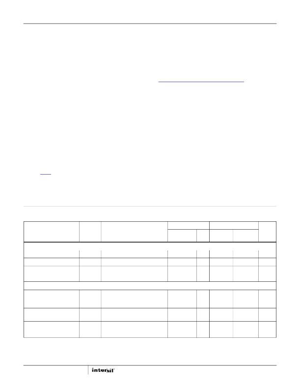
�DC� Electrical� Specifications� V� DD� =� 12V,� GND� =� 0V,� No� load� on� OUTA� or� OUTB,� unless� otherwise� specified.� Boldface� limits� apply�
�over� the� operating� junction� temperature� range,� -40°C� to� +125°C.�
�T� J� =� +25°C�
�T� J� =� -40°C� to� +125°C�
�MIN�
�MAX�
�PARAMETERS�
�SYMBOL�
�TEST� CONDITIONS�
�MIN�
�TYP�
�MAX�
�(Note� 8)�
�(Note� 8)�
�UNITS�
�POWER� SUPPLY�
�Voltage� Range� (Option� A� and� B)�
�Voltage� Range� (Option� C)�
�V� DD�
�V� DD�
�-�
�-�
�-�
�-�
�-�
�-�
�4.5�
�7.5�
�16�
�16�
�V�
�V�
�V� DD� Quiescent� Current�
�I� DD�
�ENx� =� INx� =� GND�
�INA� =� INB� =� 1MHz,� square� wave�
�-�
�-�
�5�
�25�
�-�
�-�
�-�
�-�
�-�
�mA�
�mA�
�UNDERVOLTAGE�
�VDD� Undervoltage� Lock-out�
�(Options� A� and� B)� (Note� 12,�
�Figure� 9)�
�VDD� Undervoltage� Lock-out�
�(Option� C)� (Note� 12,� Figure� 9)�
�Hysteresis� (Option� A� or� B)�
�Hysteresis� (Option� C)�
�V� UV�
�V� UV�
�ENA� =� ENB� =� True�
�INA� =� INB� =� True�
�ENA� =� ENB� =� True�
�INA� =� INB� =� True� (Note� 9)�
�-�
�-�
�-�
�-�
�3.3�
�6.5�
�~25�
�~0.95�
�-�
�-�
�-�
�-�
�-�
�-�
�-�
�-�
�-�
�-�
�-�
�-�
�V�
�V�
�mV�
�V�
�4�
�FN7707.3�
�March� 7,� 2012�
�相关PDF资料 |
PDF描述 |
|---|---|
| BYT28F-300-E3/45 | DIODE DUAL 10A 300V TO-263AB |
| ESM10DRMH | CONN EDGECARD 20POS .156 WW |
| UGB10CCTHE3/81 | DIODE 10A 150V 20NS DUAL UF |
| UGB10BCTHE3/81 | DIODE 10A 100V 20NS DUAL UF |
| EGM10DRMH | CONN EDGECARD 20POS .156 WW |
相关代理商/技术参数 |
参数描述 |
|---|---|
| ISL89165FRTBZ | 功能描述:MOSFET DRIVER 2CH 5.0V 6A 8TDFN RoHS:是 类别:集成电路 (IC) >> PMIC - MOSFET,电桥驱动器 - 外部开关 系列:- 标准包装:6,000 系列:* |
| ISL89165FRTBZ-T | 功能描述:MOSFET DRIVER 2CH 5.0V 6A 8TDFN RoHS:是 类别:集成电路 (IC) >> PMIC - MOSFET,电桥驱动器 - 外部开关 系列:- 标准包装:6,000 系列:* |
| ISL89165FRTCZ | 功能描述:MOSFET DRIVER 2CH 6A 8TDFN RoHS:是 类别:集成电路 (IC) >> PMIC - MOSFET,电桥驱动器 - 外部开关 系列:- 标准包装:6,000 系列:* |
| ISL89165FRTCZ-T | 功能描述:MOSFET DRIVER 2CH 6A 8TDFN RoHS:是 类别:集成电路 (IC) >> PMIC - MOSFET,电桥驱动器 - 外部开关 系列:- 标准包装:6,000 系列:* |
| ISL89166FBEAZ | 功能描述:IC MOSFET DRIVER 2CH 6A 8SOIC RoHS:是 类别:集成电路 (IC) >> PMIC - MOSFET,电桥驱动器 - 外部开关 系列:- 标准包装:50 系列:- 配置:高端 输入类型:非反相 延迟时间:200ns 电流 - 峰:250mA 配置数:1 输出数:1 高端电压 - 最大(自引导启动):600V 电源电压:12 V ~ 20 V 工作温度:-40°C ~ 125°C 安装类型:通孔 封装/外壳:8-DIP(0.300",7.62mm) 供应商设备封装:8-DIP 包装:管件 其它名称:*IR2127 |
发布紧急采购,3分钟左右您将得到回复。