参数资料
| 型号: | ISL9111EH30Z-T |
| 厂商: | Intersil |
| 文件页数: | 8/15页 |
| 文件大小: | 0K |
| 描述: | IC VOLTAGE REGULATOR |
| 标准包装: | 3,000 |
| 系列: | * |
�� �
�
�ISL9111,� ISL9111A�
�Typical� Application� Circuits� (Continued)�
�4.7μH�
�100�
�V� IN� = 4.2V�
�V� IN�
�4.7μF�
�6�
�3�
�1�
�SW�
�VIN�
�EN�
�VOUT�
�FB�
�5�
�4�
�V� OUT�
�5.25V�
�4.7μF�
�923k�
�90� V� IN� = 3.6V�
�80�
�70�
�60�
�V� IN� = 1.8V�
�V� IN� = 1.5V�
�GND�
�2�
�166k�
�50�
�V� IN� = 0.9V�
�ISL9111,� ISL9111A� -� ADJ�
�40�
�0.1�
�1.0�
�10�
�I� OUT� (mA)�
�100�
�1000�
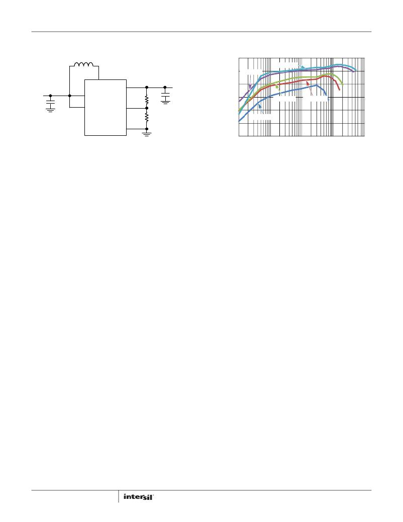
�FIGURE� 5A.� POWER� SUPPLY� SOLUTION� FOR� 5.25V� OUTPUT� VOLTAGE�
�Detailed� Description�
�Current� Mode� PWM� Operation�
�The� control� scheme� of� the� device� is� based� on� the� peak� current�
�mode� control,� and� the� control� loop� is� compensated� internally.�
�The� peak� current� of� the� N-channel� MOSFET� switch� is� sensed� to�
�limit� the� maximum� current� flowing� through� the� switch� and� the�
�inductor.� The� typical� current� limit� is� set� to� 1A.�
�The� control� circuit� includes� ramp� generator,� slope� compensator,�
��and� page� 3).� The� ramp� signal� is� derived� from� the� inductor�
�current.� This� ramp� signal� is� then� compared� to� the� error� amplifier�
�output� to� generate� the� PWM� gating� signals� for� driving� both�
�N-channel� and� P-channel� MOSFETs.� The� PWM� operation� is�
�initialized� by� the� clock� from� the� internal� oscillator� (typical�
�1.2MHz).� The� N-channel� MOSFET� is� turned� on� at� the� beginning� of�
�a� PWM� cycle,� the� P-channel� MOSFET� remains� off,� and� the� current�
�starts� ramping� up.� When� the� sum� of� the� ramp� and� the� slope�
�compensator� output� reaches� the� error� amplifier� output� voltage,�
�the� PWM� comparator� outputs� a� signal� to� turn� off� the� N-channel�
�MOSFET.� Here,� both� MOSFETs� remain� off� during� the� dead-time�
�interval,� and� then� the� P-channel� MOSFET� is� turned� on� and�
�remains� on� until� the� end� of� this� PWM� cycle.� During� this� time,� the�
�inductor� current� ramps� down� until� the� next� clock.� At� this� point,�
�following� a� short� dead� time,� the� N-channel� MOSFET� is� again�
�turned� on,� repeating� as� previously� described.�
�Skip� Mode� Operation�
�The� device� is� capable� of� operating� in� two� different� modes.� When�
�the� inductor� current� is� sensed� to� cross� zero� for� eight� consecutive�
�times,� the� converter� enters� skip� mode.� In� skip� mode,� each� pulse�
�cycle� is� still� synchronized� by� the� PWM� clock.� The� N-channel�
�MOSFET� is� turned� on� at� the� rising� edge� of� the� clock� and� turned�
�off� when� the� inductor� peak� current� reaches� typically� 25%� of� the�
�current� limit.� Then� the� P-channel� MOSFET� is� turned� on,� and� it�
�stays� on� until� its� current� goes� to� zero.� Subsequently,� both�
�N-channel� and� P-channel� MOSFETs� are� turned� off� until� the� next�
�clock� cycle� starts,� at� which� time� the� N-channel� MOSFET� is� turned�
�on� again.� When� V� OUT� is� 1.5%� typically� higher� than� the� nominal�
�output� voltage,� the� N-channel� MOSFET� is� immediately� turned� off�
�and� the� P-channel� MOSFET� is� turned� on� until� the� inductor� current�
�8�
�FIGURE� 5B.� EFFICIENCY� AT� V� OUT� =� 5.25V�
�goes� to� zero.� The� N-channel� MOSFET� resumes� operation� when�
�V� FB� falls� back� to� its� nominal� value,� repeating� the� previous�
�operation.� The� converter� returns� to� 1.2MHz� PWM� mode�
�operation� when� V� FB� drops� 1.5%� below� its� nominal� voltage.�
�Given� the� skip� mode� algorithm� incorporated� in� the� ISL9111� and�
�ISL9111A,� the� average� value� of� the� output� voltage� is�
�approximately� 0.75%� higher� than� the� nominal� output� voltage�
�under� PWM� operation.� This� positive� offset� improves� the� load�
�transient� response� when� switching� from� skip� mode� to� PWM�
�mode� operation.� The� ripple� on� the� output� voltage� is� typically�
�1.5%*V� OUT� (nominal)� when� input� voltage� is� sufficiently� lower� than�
�output� voltage,� and� it� increases� as� input� voltage� approaches�
�output� voltage.� Figure� 9� shows� the� ripple� voltage� versus� input�
�voltage.�
�Synchronous� Rectifier�
�The� ISL9111� and� ISL9111A� integrate� one� N-channel� MOSFET�
�and� one� P-channel� MOSFET� to� realize� synchronous� boost�
�converters.� Because� the� commonly� used� discrete� Schottky�
�rectifier� is� replaced� with� the� low� r� DS(ON)� P-channel� MOSFET,� the�
�power� conversion� efficiency� reaches� a� value� above� 90%.� Since� a�
�typical� step-up� converter� has� a� conduction� path� from� the� input� to�
�the� output� via� the� body� diode� of� the� P-channel� MOSFET,� a� special�
�circuit� (see� Block� Diagrams� on� page� 2� and� page� 3)� is� used� to�
�reverse� the� polarity� of� the� P-channel� body� diode� when� the� part� is�
�shut� down.� This� configuration� completely� disconnects� the� load�
�from� the� input� during� shutdown� of� the� converter.� The� benefit� of�
�this� feature� is� that� the� battery� will� not� be� completely� depleted�
�during� shutdown� of� the� converter.� No� additional� components� are�
�needed� to� disconnect� the� battery� from� the� output� of� the�
�converter.�
�Minimum� Startup� and� Minimum� Operating�
�Voltage�
�The� ISL9111� and� ISL9111A� address� applications� with�
�rechargeable� and� non-rechargeable� battery� cells.�
�1.� The� ISL9111� has� a� UVLO� feature.� The� part� can� start� up� with� a�
�0.8V� typical� input� voltage� and� internally� shut� off� when� the�
�battery� drops� below� 0.7V� to� protect� a� rechargeable� battery�
�from� over-discharge.�
�FN7602.4�
�June� 4,� 2012�
�相关PDF资料 |
PDF描述 |
|---|---|
| ISL9112IRT7Z-T7A | IC REG BUCK BOOST SYNC 5V 12TDFN |
| ISL9217IRZ | IC MULTI-CELL LI-ION PROT 24-QFN |
| ISL9443IRZ-T7A | IC REG CTRLR BUCK PWM CM 32-QFN |
| ISL9444IRZ | IC REG CTRLR BUCK PWM CM 40-QFN |
| ISL9491ERZ | IC REG SGL LNB CONTROL 16QFN |
相关代理商/技术参数 |
参数描述 |
|---|---|
| ISL9111EH30Z-T7A | 功能描述:IC REG BOOST SYNC 3V 1A 6SOT23-6 RoHS:是 类别:集成电路 (IC) >> PMIC - 稳压器 - DC DC 开关稳压器 系列:- 标准包装:1 系列:EZBuck™ 类型:降压(降压) 输出类型:可调式 输出数:1 输出电压:0.8 V ~ 22.1 V 输入电压:3 V ~ 26 V PWM 型:电流模式 频率 - 开关:1.5MHz 电流 - 输出:1.8A 同步整流器:无 工作温度:-40°C ~ 85°C 安装类型:表面贴装 封装/外壳:8-WFDFN 裸露焊盘 包装:剪切带 (CT) 供应商设备封装:8-DFN(2x2) 其它名称:785-1276-1 |
| ISL9111EH33Z-T | 功能描述:IC VOLTAGE REGULATOR RoHS:是 类别:集成电路 (IC) >> PMIC - 稳压器 - DC DC 开关稳压器 系列:* 标准包装:50 系列:- 类型:升压(升压) 输出类型:可调式 输出数:1 输出电压:5 V ~ 25 V 输入电压:2.3 V ~ 5.5 V PWM 型:电流模式 频率 - 开关:600kHz,1.2MHz 电流 - 输出:1A 同步整流器:无 工作温度:-40°C ~ 85°C 安装类型:表面贴装 封装/外壳:8-TSSOP,8-MSOP(0.118",3.00mm 宽) 包装:管件 供应商设备封装:8-MSOP |
| ISL9111EH33Z-T7A | 功能描述:IC REG BST SYNC 3.3V 1A 6SOT23-6 RoHS:是 类别:集成电路 (IC) >> PMIC - 稳压器 - DC DC 开关稳压器 系列:- 标准包装:1 系列:EZBuck™ 类型:降压(降压) 输出类型:可调式 输出数:1 输出电压:0.8 V ~ 22.1 V 输入电压:3 V ~ 26 V PWM 型:电流模式 频率 - 开关:1.5MHz 电流 - 输出:1.8A 同步整流器:无 工作温度:-40°C ~ 85°C 安装类型:表面贴装 封装/外壳:8-WFDFN 裸露焊盘 包装:剪切带 (CT) 供应商设备封装:8-DFN(2x2) 其它名称:785-1276-1 |
| ISL9111EH50Z-T | 功能描述:IC VOLTAGE REGULATOR RoHS:是 类别:集成电路 (IC) >> PMIC - 稳压器 - DC DC 开关稳压器 系列:* 标准包装:50 系列:- 类型:升压(升压) 输出类型:可调式 输出数:1 输出电压:5 V ~ 25 V 输入电压:2.3 V ~ 5.5 V PWM 型:电流模式 频率 - 开关:600kHz,1.2MHz 电流 - 输出:1A 同步整流器:无 工作温度:-40°C ~ 85°C 安装类型:表面贴装 封装/外壳:8-TSSOP,8-MSOP(0.118",3.00mm 宽) 包装:管件 供应商设备封装:8-MSOP |
| ISL9111-EH50Z-T7A | 制造商:Intersil Corporation 功能描述: |
发布紧急采购,3分钟左右您将得到回复。