- 您现在的位置:买卖IC网 > PDF目录20613 > ISL9305IRTAANLZ-T (Intersil)IC REG QD BUCK/LINEAR 16TQFN PDF资料下载
参数资料
| 型号: | ISL9305IRTAANLZ-T |
| 厂商: | Intersil |
| 文件页数: | 3/17页 |
| 文件大小: | 771K |
| 描述: | IC REG QD BUCK/LINEAR 16TQFN |
| 产品培训模块: | Patient Monitoring and Diagnostic Equipment Solutions |
| 标准包装: | 6,000 |
| 拓扑: | 降压(降压)(2),线性(LDO)(2) |
| 功能: | 任何功能 |
| 输出数: | 4 |
| 频率 - 开关: | 3MHz |
| 电压/电流 - 输出 1: | 0.8 V ~ 5.5 V,800mA |
| 电压/电流 - 输出 2: | 0.8 V ~ 5.5 V,800mA |
| 电压/电流 - 输出 3: | 0.9 V ~ 3.3 V,350mA |
| 带 LED 驱动器: | 无 |
| 带监控器: | 无 |
| 带序列发生器: | 无 |
| 电源电压: | 1.5 V ~ 5.5 V |
| 工作温度: | -40°C ~ 85°C |
| 安装类型: | 表面贴装 |
| 封装/外壳: | 16-WQFN 裸露焊盘 |
| 供应商设备封装: | 16-TQFN-EP(4x4) |
| 包装: | 带卷 (TR) |
ISL9305
3
FN7605.1
August 15, 2011
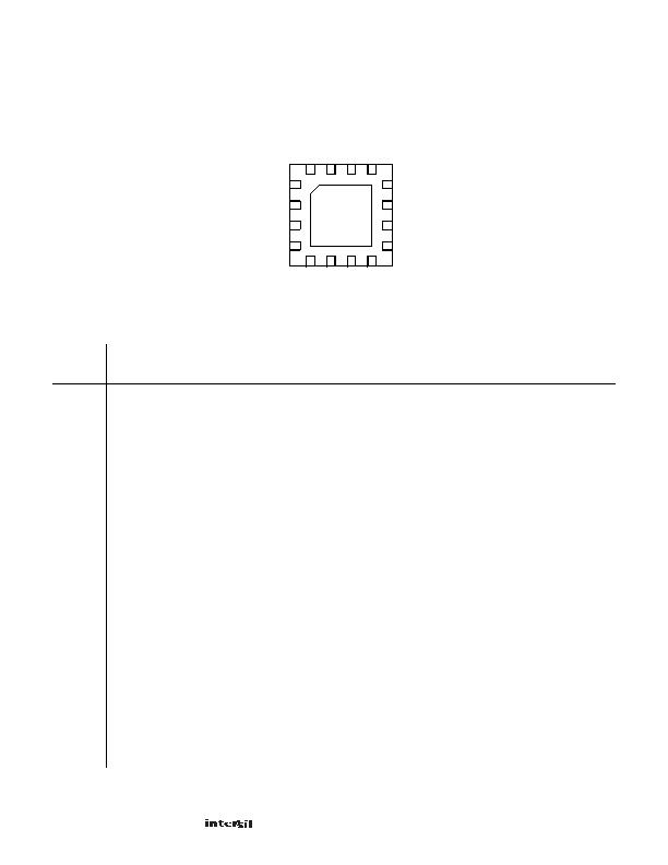
Pin Configuration
ISL9305
(16 LD 4X4 TQFN)
TOP VIEW
E-PAD
1
2
3
4
5
6
7
8
9
10
11
12
13
14
15
16
SCLK
VINDCD1
DCDPG
FB2
VINDCD2
FB1
SDAT
GNDLDO
Pin Descriptions
PIN
NUMBER
(TQFN)
NAME
DESCRIPTION
1
VINDCD1
Input voltage for buck converter DCD1 and it also serves as the power supply pin for the whole internal digital/ analog
circuits.
2
FB1
Feedback pin for DCD1, connect external voltage divider resistors between DCDC1 output, this pin and ground. For
fixed output versions, connect this pin directly to the DCD1 output.
3
SCLK
I
2
C interface clock pin.
4
SDAT
I
2
C interface data pin.
5
VINLDO1
Input voltage for LDO1.
6
VOLDO1
Output voltage of LDO1.
7
VOLDO2
Output voltage of LDO2.
8
VINLDO2
Input voltage for LDO2.
9
GNDLDO
Power ground for LDO1 and LDO2.
10
DCDPG
The DCDPG pin is an open-drain output to indicate the state of the DCD1/DCD2 output voltages. When both DCD1
and DCD2 are enabled, the output is released to be pulled high by an external pull-up resistor if both converter
voltages are within the power-good range. The pin will be pulled low if either DCD is outside their range. When only
one DCD is enabled, the state of the enabled DCDs output will define the state of the DCDPG pin. The DCDPG state
can be programmed for a delay of up to 200ms before being released to rise high. The programming range is
1ms~200ms through the I
2
C interface.
11
FB2
Feedback pin for DCD2, connect external voltage divider resistors between DCD2 output, this pin and ground. For
fixed output versions, connect this pin directly to the DCD2 output.
12
VINDCD2
Input voltage for buck converter DCD2.
13
SW2
Switching node for DCD2, connect to one terminal of the inductor.
14
GNDDCD2
Power ground for DCD2.
15
GNDDCD1
Power ground for DCD1.
16
SW1
Switching node for DCD1, connect to one terminal of the inductor.
E-pad
E-pad
Exposed Pad. Connect to system ground.
相关PDF资料 |
PDF描述 |
|---|---|
| ISL6442IAZ | IC REG TRPL BCK/LINEAR 24QSOP |
| ISL6442IAZ-TK | IC REG TRPL BCK/LINEAR 24QSOP |
| AGM28DTMH | CONN EDGECARD 56POS R/A .156 SLD |
| ECC28DCMS | CONN EDGECARD 56POS .100 WW |
| AGM28DTMD | CONN EDGECARD 56POS R/A .156 SLD |
相关代理商/技术参数 |
参数描述 |
|---|---|
| ISL9305IRTBCNLZ-T | 功能描述:电流型 PWM 控制器 DL DC/DC & DLLDO /1 8/1 2/3 TQFN L16 RoHS:否 制造商:Texas Instruments 开关频率:27 KHz 上升时间: 下降时间: 工作电源电压:6 V to 15 V 工作电源电流:1.5 mA 输出端数量:1 最大工作温度:+ 105 C 安装风格:SMD/SMT 封装 / 箱体:TSSOP-14 |
| ISL9305IRTBFNCZ-T | 功能描述:电流型 PWM 控制器 DL DC/DC & DLLDO /1 8/1 2/3 TQFN L16 RoHS:否 制造商:Texas Instruments 开关频率:27 KHz 上升时间: 下降时间: 工作电源电压:6 V to 15 V 工作电源电流:1.5 mA 输出端数量:1 最大工作温度:+ 105 C 安装风格:SMD/SMT 封装 / 箱体:TSSOP-14 |
| ISL9305IRTHAANLZ-T | 功能描述:电流型 PWM 控制器 DL DC/DC & DLLDO /1 8/1 2/3 TQFN L16 RoHS:否 制造商:Texas Instruments 开关频率:27 KHz 上升时间: 下降时间: 工作电源电压:6 V to 15 V 工作电源电流:1.5 mA 输出端数量:1 最大工作温度:+ 105 C 安装风格:SMD/SMT 封装 / 箱体:TSSOP-14 |
| ISL9305IRTHBCNLZ-T | 功能描述:电流型 PWM 控制器 DL DC/DC & DLLDO /1 8/1 2/3 TQFN L16 RoHS:否 制造商:Texas Instruments 开关频率:27 KHz 上升时间: 下降时间: 工作电源电压:6 V to 15 V 工作电源电流:1.5 mA 输出端数量:1 最大工作温度:+ 105 C 安装风格:SMD/SMT 封装 / 箱体:TSSOP-14 |
| ISL9305IRTHBFNCZ-T | 功能描述:电流型 PWM 控制器 DL DC/DC & DLLDO /1 8/1 2/3 TQFN L16 RoHS:否 制造商:Texas Instruments 开关频率:27 KHz 上升时间: 下降时间: 工作电源电压:6 V to 15 V 工作电源电流:1.5 mA 输出端数量:1 最大工作温度:+ 105 C 安装风格:SMD/SMT 封装 / 箱体:TSSOP-14 |
发布紧急采购,3分钟左右您将得到回复。