参数资料
| 型号: | ISL96017WIRT8Z-T |
| 厂商: | Intersil |
| 文件页数: | 2/13页 |
| 文件大小: | 0K |
| 描述: | IC XDCP 128-TAP 10KOHM 8-TDFN |
| 标准包装: | 6,000 |
| 接片: | 128 |
| 电阻(欧姆): | 10k |
| 电路数: | 1 |
| 温度系数: | 标准值 ±100 ppm/°C |
| 存储器类型: | 非易失 |
| 接口: | I²C |
| 电源电压: | 3 V ~ 3.6 V |
| 工作温度: | -40°C ~ 85°C |
| 安装类型: | 表面贴装 |
| 封装/外壳: | 8-WDFN 裸露焊盘 |
| 供应商设备封装: | 8-TDFN(3x3) |
| 包装: | 带卷 (TR) |
ISL96017
10
FN8243.2
June 8, 2012
Write Operation
A Write operation requires a START condition, followed by a valid
Identification Byte, a valid Address Byte, one or more Data Bytes,
and a STOP condition (See Figure 9). After each of the bytes, this
device responds with an ACK. At this time, if the operation is only
writing to volatile registers, then the device enters its standby
state. If one or more Data Bytes are to be written to non-volatile
memory, the device begins its internal write cycle to non-volatile
memory. During this cycle, the device ignores transitions at the
SDA and SCL pins, and the SDA output is at a high impedance
state. When the internal non-volatile write cycle is completed, the
device enters its standby state.
The memory is organized as 128 pages of 16 bytes each. This
allows writing 16 bytes on a single I2C interface operation,
followed by a single internal non-volatile write cycle. The
addresses of bytes within a page share the same eight MSBs,
and differ on the four LSBs. For example, the first page is located
at addresses 0 hex through F hex, the second page is located at
addresses 10 hex through 1F hex, etc.
A Write operation with more than one Data Byte sends the first
Data Byte to the memory address indicated by the three address
bits of the Identification Byte plus the eight bits of the Address
Byte, the second Data Byte to the following address, etc.
A single Write operation has to stay within a page. If the Address
Byte corresponds to the lowest address of a page, then the Write
operation can have anywhere from 1 to 16 Data Bytes. If the
Address Byte corresponds to the highest address of a page, then
only one byte can be written with that Write operation.
See “Access to DCP Register and IVR” for additional information.
Data Protection
The WP pin has to be at logic HIGH to perform any Write
operation to the device. When WP is active (LOW) the device
ignores Data Bytes of a Write operation, does not respond to
them with ACK, and instead, goes to its standby state waiting for
a new START condition.
A valid Identification Byte, Address Byte, and total number of SCL
pulses act as a protection of both volatile and non-volatile
registers.
During a Write sequence, Data Bytes are loaded into an internal
shift register as they are received. If the address bits in the
Identification Byte plus the bits in the Address Byte are all ones,
the Data Byte is transferred to the DCP Register at the falling
edge of the SCL pulse that loads the last bit (LSB) of the Data
Byte.
The STOP condition acts as a protection of non-volatile memory.
Non-volatile internal write cycles are started by STOP conditions.
Read Operation
A Read operation consist of a three byte instruction followed by
one or more Data Bytes (See Figure 10). The master initiates the
operation issuing the following sequence: a START, the
Identification Byte with the R/W bit set to “0”, an Address Byte
which contains the LSBs of the memory address, a second
START, and a second Identification Byte with the same address
bits but with the R/W bit set to “1”. After each of the three bytes,
this device responds with an ACK. Then this device transmits
Data Bytes as long as the master responds with an ACK during
the SCL cycle following the eighth bit of each byte. The master
terminates the Read operation (issuing a STOP condition)
following the last bit of the last Data Byte. The Data Bytes are
from the memory location indicated by an internal pointer. This
pointer initial value is determined by the address bits in the
Identification Byte plus the bits in the Address Byte in the Read
operation instruction, and increments by one during
transmission of each Data Byte.
SDA OUTPUT FROM
TRANSMITTER
SDA OUTPUT FROM
RECEIVER
8
1
9
START
ACK
SCL FROM MASTER
HIGH IMPEDANCE
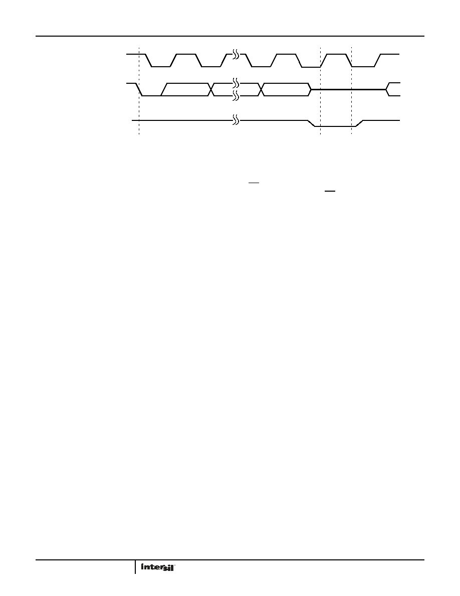
FIGURE 8. ACKNOWLEDGE RESPONSE FROM RECEIVER
相关PDF资料 |
PDF描述 |
|---|---|
| MS3106E24-58S | CONN PLUG 13POS STRAIGHT W/SCKT |
| VI-BTL-MW-B1 | CONVERTER MOD DC/DC 28V 100W |
| VI-26D-MY-F3 | CONVERTER MOD DC/DC 85V 50W |
| ISL96017UIRT8Z-TK | IC XDCP 128-TAP 50KOHM 8-TDFN |
| VI-BTL-MV | CONVERTER MOD DC/DC 28V 150W |
相关代理商/技术参数 |
参数描述 |
|---|---|
| ISL96017WIRT8Z-TK | 功能描述:IC XDCP 128-TAP 10KOHM 8-TDFN RoHS:是 类别:集成电路 (IC) >> 数据采集 - 数字电位器 系列:- 产品培训模块:Lead (SnPb) Finish for COTS Obsolescence Mitigation Program 标准包装:2,500 系列:- 接片:256 电阻(欧姆):100k 电路数:2 温度系数:标准值 35 ppm/°C 存储器类型:易失 接口:6 线串行(芯片选择,递增,增/减) 电源电压:2.6 V ~ 5.5 V 工作温度:-40°C ~ 125°C 安装类型:表面贴装 封装/外壳:14-TSSOP(0.173",4.40mm 宽) 供应商设备封装:14-TSSOP 包装:带卷 (TR) |
| ISL97516IUZ | 功能描述:直流/直流开关转换器 600KHZ/1.2MHZ PWM ST EP-UP REG 8LD RoHS:否 制造商:STMicroelectronics 最大输入电压:4.5 V 开关频率:1.5 MHz 输出电压:4.6 V 输出电流:250 mA 输出端数量:2 最大工作温度:+ 85 C 安装风格:SMD/SMT |
| ISL97516IUZEVALZ | 制造商:Intersil Corporation 功能描述:ISL97516IUZ EVALUATION BOARD - 8LD MSOP - ROHS COMPLIANT - Bulk 制造商:Intersil Corporation 功能描述:EVALUATION BOARD FOR ISL97516IUZ 制造商:Intersil 功能描述:ISL97516IUZ EVALI ON BRD 8LD RHS CMPL |
| ISL97516IUZ-EVALZ | 功能描述:EVALUATION BOARD FOR ISL97516IUZ RoHS:是 类别:编程器,开发系统 >> 评估板 - DC/DC 与 AC/DC(离线)SMPS 系列:- 产品培训模块:Obsolescence Mitigation Program 标准包装:1 系列:True Shutdown™ 主要目的:DC/DC,步升 输出及类型:1,非隔离 功率 - 输出:- 输出电压:- 电流 - 输出:1A 输入电压:2.5 V ~ 5.5 V 稳压器拓扑结构:升压 频率 - 开关:3MHz 板类型:完全填充 已供物品:板 已用 IC / 零件:MAX8969 |
| ISL97516IUZ-T | 功能描述:IC REG BOOST ADJ 1A 8MSOP RoHS:是 类别:集成电路 (IC) >> PMIC - 稳压器 - DC DC 开关稳压器 系列:- 标准包装:50 系列:- 类型:升压(升压) 输出类型:可调式 输出数:1 输出电压:5 V ~ 25 V 输入电压:2.3 V ~ 5.5 V PWM 型:电流模式 频率 - 开关:600kHz,1.2MHz 电流 - 输出:1A 同步整流器:无 工作温度:-40°C ~ 85°C 安装类型:表面贴装 封装/外壳:8-TSSOP,8-MSOP(0.118",3.00mm 宽) 包装:管件 供应商设备封装:8-MSOP |
发布紧急采购,3分钟左右您将得到回复。