- 您现在的位置:买卖IC网 > PDF目录13665 > ISL97519AIUZ-T (Intersil)IC REG BOOST ADJ 1A 8MSOP PDF资料下载
参数资料
| 型号: | ISL97519AIUZ-T |
| 厂商: | Intersil |
| 文件页数: | 6/9页 |
| 文件大小: | 0K |
| 描述: | IC REG BOOST ADJ 1A 8MSOP |
| 标准包装: | 2,500 |
| 类型: | 升压(升压) |
| 输出类型: | 可调式 |
| 输出数: | 1 |
| 输出电压: | 5 V ~ 25 V |
| 输入电压: | 2.3 V ~ 5.5 V |
| PWM 型: | 电流模式 |
| 频率 - 开关: | 600kHz,1.2MHz |
| 电流 - 输出: | 1A |
| 同步整流器: | 无 |
| 工作温度: | -40°C ~ 85°C |
| 安装类型: | 表面贴装 |
| 封装/外壳: | 8-TSSOP,8-MSOP(0.118",3.00mm 宽) |
| 包装: | 带卷 (TR) |
| 供应商设备封装: | 8-MSOP |
�� �
�
�ISL97519A�
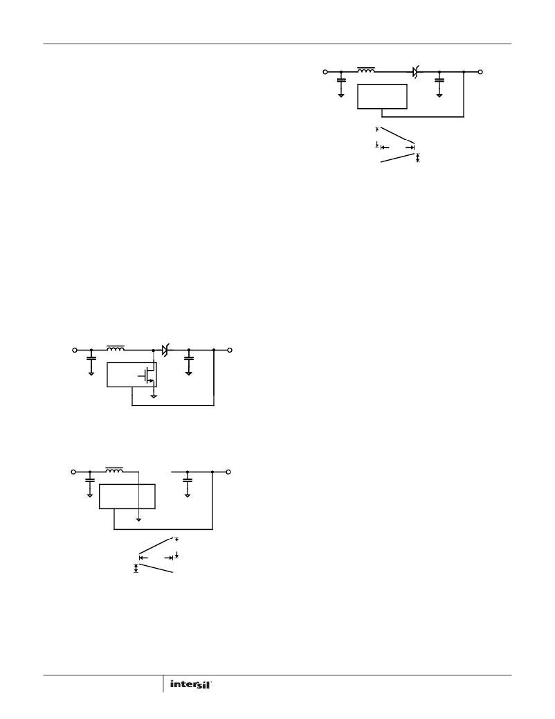
�During� the� second� cycle,� the� power� FET� turns� off� and� the�
�Schottky� diode� is� forward� biased,� (see� Figure� 13).� The� energy�
�stored� in� the� inductor� is� pumped� to� the� output� supplying�
�output� current� and� charging� the� output� capacitor.� The� Schottky�
�V� IN�
�C� IN�
�L�
�D�
�C� OUT�
�V� OUT�
�Δ� I� L� =� Δ� T2� ×� ----------------------------�
�Δ� T2� =� -------------�
�F� SW�
�Δ� I� L2�
�D� V� IN� 1� –� D� V� IN� –� V� OUT�
�-----------� � --------� +� -------------� � ----------------------------� =� 0�
�F� SW�
�F� SW�
�diode� side� of� the� inductor� is� clamped� to� a� Schottky� diode�
�above� the� output� voltage.� So� the� voltage� drop� across� the�
�inductor� is� V� IN� -� V� OUT� .� The� change� in� inductor� current� during� the�
�second� cycle� is� shown� in� Equation� 2:�
�V� IN� –� V� OUT�
�L�
�1� –� D�
�(EQ.� 2)�
�For� stable� operation,� the� same� amount� of� energy� stored� in� the�
�inductor� must� be� taken� out.� The� change� in� inductor� current�
�during� the� two� cycles� must� be� the� same,� as� shown� in�
�Equation� 3.�
�Δ� I1� +� Δ� I2� =� 0�
�L� L�
�ISL97519A�
�I� L�
�Δ� T� 2�
�Δ� V� O�
�FIGURE� 13.� BOOST� CONVERTER� -� CYCLE� 2,� POWER� SWITCH�
�OPEN�
�Output� Voltage�
�An� external� feedback� resistor� divider� is� required� to� divide� the�
�output� voltage� down� to� the� nominal� 1.24V� reference� voltage.�
�The� current� drawn� by� the� resistor� network� should� be� limited� to�
�maintain� the� overall� converter� efficiency.� The� maximum� value�
�of� the� resistor� network� is� limited� by� the� feedback� input� bias�
�current� and� the� potential� for� noise� being� coupled� into� the�
�feedback� pin.� A� resistor� network� less� than� 100k� is�
�V� OUT� 1�
�1� –� D�
�V� IN�
�V� OUT� =� V� FB� � ?� ?�
�?� R� 1� ?�
�R� 2� ?�
�-------------� =� -------------�
�L�
�D�
�(EQ.� 3)�
�recommended.� The� boost� converter� output� voltage� is�
�determined� by� the� relationship� in� Equation� 4:�
�1� +� -------�
�?�
�The� nominal� VFB� voltage� is� 1.24V.�
�(EQ.� 4)�
�V� IN�
�C� IN�
�C� OUT�
�V� OUT�
�Inductor� Selection�
�The� inductor� selection� determines� the� output� ripple� voltage,�
�ISL97519A�
�FIGURE� 11.� BOOST� CONVERTER�
�transient� response,� output� current� capability,� and� efficiency.� Its�
�selection� depends� on� the� input� voltage,� output� voltage,�
�switching� frequency,� and� maximum� output� current.� For� most�
�applications,� the� inductance� should� be� in� the� range� of� 2μH� to�
�33μH.� The� inductor� maximum� DC� current� specification� must�
�be� greater� than� the� peak� inductor� current� required� by� the�
�regulator.The� peak� inductor� current� can� be� calculated� in�
�Equation� 5:�
�I� L� (� PEAK� )� =� -------------------------------� +� 1� ?� 2� � -----------------------------------------------�
�V� IN�
�C� IN�
�L�
�C� OUT�
�V� OUT�
�I� OUT� ×� V� OUT� V� IN� ×� (� V� OUT� –� V� IN� )�
�V� IN� L� � V� OUT� � FREQ�
�(EQ.� 5)�
�Δ� I� L1�
�Δ� V� O� =� ------------------------� +� I� OUT� ×� ESR�
�ISL97519A�
�I� L�
�Δ� T� 1�
�Δ� V� O�
�FIGURE� 12.� BOOST� CONVERTER� -� CYCLE� 1,� POWER� SWITCH�
�CLOSE�
�6�
�Output� Capacitor�
�Low� ESR� capacitors� should� be� used� to� minimized� the� output�
�voltage� ripple.� Multi-layer� ceramic� capacitors� (X5R� and� X7R)�
�are� preferred� for� the� output� capacitors� because� of� their� lower�
�ESR� and� small� packages.� Tantalum� capacitors� with� higher� ESR�
�can� also� be� used.� The� output� ripple� can� be� calculated� as� shown�
�in� Equation� 6:�
�I� OUT� � D� (EQ.� 6)�
�F� SW� � C� O�
�For� noise� sensitive� application,� a� 0.1μF� placed� in� parallel� with�
�the� larger� output� capacitor� is� recommended� to� reduce� the�
�switching� noise� coupled� from� the� LX� switching� node.�
�FN6683.3�
�February� 16,� 2012�
�相关PDF资料 |
PDF描述 |
|---|---|
| MAX6728AKASYD3+T | IC SUPERVISOR MPU SOT23-8 |
| PM3604-25-B-RC | INDUCTOR DUAL TOROID 25UH SMD |
| MAX6729AKAZGD3+T | IC SUPERVISOR MPU SOT23-8 |
| MAX6727KASVD3+T | IC SUPERVISOR MPU SOT23-8 |
| MAX6729AKAVDD3+T | IC SUPERVISOR MPU SOT23-8 |
相关代理商/技术参数 |
参数描述 |
|---|---|
| ISL97519AIUZ-TK | 功能描述:IC REG BOOST ADJ 1A 8MSOP RoHS:是 类别:集成电路 (IC) >> PMIC - 稳压器 - DC DC 开关稳压器 系列:- 产品培训模块:Lead (SnPb) Finish for COTS Obsolescence Mitigation Program 标准包装:2,500 系列:- 类型:降压(降压) 输出类型:两者兼有 输出数:1 输出电压:5V,1 V ~ 10 V 输入电压:3.5 V ~ 28 V PWM 型:电流模式 频率 - 开关:220kHz ~ 1MHz 电流 - 输出:600mA 同步整流器:无 工作温度:-40°C ~ 125°C 安装类型:表面贴装 封装/外壳:16-SSOP(0.154",3.90mm 宽) 包装:带卷 (TR) 供应商设备封装:16-QSOP |
| ISL97519IUZ | 功能描述:IC REG BOOST ADJ 1A 8MSOP RoHS:是 类别:集成电路 (IC) >> PMIC - 稳压器 - DC DC 开关稳压器 系列:- 标准包装:50 系列:- 类型:升压(升压) 输出类型:可调式 输出数:1 输出电压:5 V ~ 25 V 输入电压:2.3 V ~ 5.5 V PWM 型:电流模式 频率 - 开关:600kHz,1.2MHz 电流 - 输出:1A 同步整流器:无 工作温度:-40°C ~ 85°C 安装类型:表面贴装 封装/外壳:8-TSSOP,8-MSOP(0.118",3.00mm 宽) 包装:管件 供应商设备封装:8-MSOP |
| ISL97519IUZEVALZ | 功能描述:EVAL BOARD FOR ISL97519IUZ RoHS:是 类别:编程器,开发系统 >> 评估板 - DC/DC 与 AC/DC(离线)SMPS 系列:* 标准包装:1 系列:- 主要目的:DC/DC,步降 输出及类型:1,非隔离 功率 - 输出:- 输出电压:3.3V 电流 - 输出:3A 输入电压:4.5 V ~ 28 V 稳压器拓扑结构:降压 频率 - 开关:250kHz 板类型:完全填充 已供物品:板 已用 IC / 零件:L7981 其它名称:497-12113STEVAL-ISA094V1-ND |
| ISL97519IUZ-T | 功能描述:IC REG BOOST ADJ 1A 8MSOP RoHS:是 类别:集成电路 (IC) >> PMIC - 稳压器 - DC DC 开关稳压器 系列:- 产品培训模块:Lead (SnPb) Finish for COTS Obsolescence Mitigation Program 标准包装:2,500 系列:- 类型:降压(降压) 输出类型:两者兼有 输出数:1 输出电压:5V,1 V ~ 10 V 输入电压:3.5 V ~ 28 V PWM 型:电流模式 频率 - 开关:220kHz ~ 1MHz 电流 - 输出:600mA 同步整流器:无 工作温度:-40°C ~ 125°C 安装类型:表面贴装 封装/外壳:16-SSOP(0.154",3.90mm 宽) 包装:带卷 (TR) 供应商设备封装:16-QSOP |
| ISL97519IUZ-TK | 功能描述:IC REG BOOST ADJ 1A 8MSOP RoHS:是 类别:集成电路 (IC) >> PMIC - 稳压器 - DC DC 开关稳压器 系列:- 产品培训模块:Lead (SnPb) Finish for COTS Obsolescence Mitigation Program 标准包装:2,500 系列:- 类型:降压(降压) 输出类型:两者兼有 输出数:1 输出电压:5V,1 V ~ 10 V 输入电压:3.5 V ~ 28 V PWM 型:电流模式 频率 - 开关:220kHz ~ 1MHz 电流 - 输出:600mA 同步整流器:无 工作温度:-40°C ~ 125°C 安装类型:表面贴装 封装/外壳:16-SSOP(0.154",3.90mm 宽) 包装:带卷 (TR) 供应商设备封装:16-QSOP |
发布紧急采购,3分钟左右您将得到回复。