- 您现在的位置:买卖IC网 > PDF目录20796 > ISL97634IRT18Z-T (Intersil)IC LED DRIVR WHITE BCKLGT 8-TDFN PDF资料下载
参数资料
| 型号: | ISL97634IRT18Z-T |
| 厂商: | Intersil |
| 文件页数: | 9/12页 |
| 文件大小: | 0K |
| 描述: | IC LED DRIVR WHITE BCKLGT 8-TDFN |
| 标准包装: | 6,000 |
| 拓扑: | PWM,升压(升压) |
| 输出数: | 1 |
| 内部驱动器: | 是 |
| 类型 - 主要: | 车载,背光 |
| 类型 - 次要: | 白色 LED |
| 频率: | 1.3MHz ~ 1.6MHz |
| 电源电压: | 2.4 V ~ 5.5 V |
| 安装类型: | 表面贴装 |
| 封装/外壳: | 8-WFDFN 裸露焊盘 |
| 供应商设备封装: | 8-TDFN(2x3) |
| 包装: | 带卷 (TR) |
| 工作温度: | -40°C ~ 85°C |
�� �
�
�ISL97634�
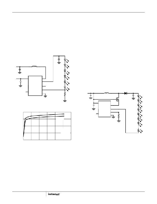
�Efficiency� Improvement�
�Figure� 2� shows� the� efficiency� measurements� during� PWM�
�operation.� The� choice� of� the� inductor� has� a� significant� impact� on�
�the� power� efficiency.� Equation� 4� shows� the� higher� the� inductance,�
�the� lower� the� peak� current,� therefore,� the� lower� the� conduction�
�and� switching� losses.� On� the� other� hand,� it� has� also� a� higher� series�
�resistance.� Nevertheless,� the� efficiency� improvement� effect� by�
�lowering� the� peak� current� is� greater� than� the� resistance� increases�
�with� larger� value� of� inductor.� Efficiency� can� also� be� improved� for�
�systems� that� have� high� supply� voltages.� Since� the� ISL97634� can�
�only� supply� from� 2.4V� to� 5.5V,� V� IN� must� be� separated� from� the�
�high� supply� voltage� for� the� boost� circuit� as� shown� in� Figure� 16� and�
�the� efficiency� improvement� is� shown� in� Figure� 17.�
�follower� action� of� M1,� limiting� the� maximum� voltage� on� the�
�ISL97634� LX� pin� to� below� V� IN� ,� but� allowing� the� output� voltage� to� go�
�much� higher� than� the� breakdown� limit� on� the� LX� pin.� The� switch�
�current� limit� and� maximum� duty� cycle� will� not� be� changed� by� this�
�setup,� so� input� voltage� will� need� to� be� carefully� considered� to� make�
�sure� that� the� required� output� voltage� and� current� levels� are�
�achievable.� Because� the� source� of� M1� is� effectively� floating� when�
�the� internal� LX� switch� is� off,� the� drain-to-source� capacitance� of� M1�
�may� be� sufficient� to� capacitively� pull� the� node� high� enough� to� break�
�down� the� gate� oxide� of� M1.� To� prevent� this,� V� OUT� should� be�
�connected� to� V� IN� ,� allowing� the� internal� Schottky� diode� to� limit� the�
�peak� voltage.� This� will� also� hold� the� VOUT� pin� at� a� known� low�
�voltage,� preventing� the� built� in� OVP� function� from� causing� problems.�
�This� OVP� function� is� effectively� useless� in� this� mode� as� the� real�
�C3� 0.22μF�
�D1�
�output� voltage� is� outside� its� intended� range.� If� the� user� wants� to�
�implement� their� own� OVP� protection� (to� prevent� damage� to� the�
�output� capacitor),� they� should� insert� a� zener� diode� from� VOUT� to� the�
�Vs� =� 12V�
�C1�
�1μF�
�1�
�L1�
�22μH�
�2�
�D2�
�D3�
�FB� pin.� In� this� setup,� it� would� be� wise� not� to� use� the� FBSW� to� FB�
�switch,� as� otherwise,� the� zener� diode� will� have� to� be� a� high� power�
�one� capable� of� dissipating� the� entire� LED� load� power.� Then� the� LED�
�V� IN� =� 2.7V� TO� 5.5V�
�C2� 0.1μF�
�VIN� LX�
�VOUT�
�ISL97634�
�FBSW�
�D4�
�D5�
�D6�
�stack� can� then� be� connected� directly� to� the� sense� resistor� via� a�
�10k� Ω� resistor� to� FB.� A� zener� can� be� placed� from� VOUT� to� the� FB� pin�
�allowing� an� overvoltage� event� to� pull-up� on� FB� with� a� low�
�breakdown� current� (and� thus� low� power� zener� diode)� as� a� result�
�of� the� 10k� Ω� resistor.�
�PWM� /� EN�
�FB�
�GND�
�R1�
�4� Ω�
�V� IN� =� 2.7V� TO� 5.5V�
�C1�
�1μF�
�L1�
�1� 2�
�10μH� or� 22μH�
�M1�
�D0�
�10BQ100�
�C3� 4.7μF�
�FQT13N06L�
�FIGURE� 16.� SEPARATE� HIGH� INPUT� VOLTAGE� FOR� HIGHER�
�EFFICIENCY� OPERATION�
�C2�
�0.1μF�
�VIN� VOUT�
�LX�
�ISL97634�
�SK011C226KAR�
�FBSW�
�.�
�90�
�V� S� = 12V�
�FB�
�PWM/EN�
�GND�
�R1�
�6.3� Ω�
�85�
�V� S� = 9V�
�80�
�V� IN� =� 4V�
�75�
�7� LEDs�
�L1� =� 22μH�
�R1� =� 4� Ω�
�f� PWM�
�FIGURE� 18.� HIGH� VOLTAGE� LED� DRIVER� USING� A� CASCODE�
�70�
�0�
�5�
�10�
�15�
�20�
�25�
�30�
�SEPIC� Operation�
�ILED� (mA)�
�FIGURE� 17.� EFFICIENCY� IMPROVEMENT� WITH� 9� AND� 12V� INPUTS�
�Operation� with� VOUT� above� 26V�
�For� LED� backlighting� applications� that� need� an� output� voltage� above�
�26V,� the� voltage� range� of� the� ISL97634� is� not� sufficient.� However,�
�the� ISL97634� can� be� used� as� an� LED� controller� with� an� external�
�protection� MOSFET� connected� in� cascode� fashion� to� achieve� higher�
�output� voltage� as� shown� in� Figure� 18.� A� 60V� logic� level� N-Channel�
�MOSFET� is� configured� such� that� its� drain� ties� between� the� inductor�
�and� the� anode� of� Schottky� diode,� its� gate� ties� to� the� input,� and� its�
�source� ties� to� the� ISL97634� LX� node� connecting� to� the� drain� of� the�
�internal� switch.� When� the� internal� switch� turns� on,� it� pulls� the� source�
�of� M1� down� to� ground� and� LX� conducts� as� normal.� When� the�
�internal� switch� turns� off,� the� source� of� M1� will� be� pulled� up� by� the�
�9�
�For� applications� where� the� output� voltage� is� not� always� above� the�
�input� voltage,� a� buck� or� boost� regulation� is� needed.� A� SEPIC�
�(Single-Ended� Primary� Inductance� Converter)� topology,� shown� in�
�Figure� 19,� can� be� considered� for� such� an� application.� A� single�
�cell� Li-ion� battery� operating� a� cellular� phone� backlight� or�
�flashlight� is� one� example.� The� battery� voltage� is� between� 2.5V�
�and� 4.2V,� depending� on� the� state� of� charge.� On� the� other� hand,�
�the� output� may� require� only� one� 3V� to� 4V� medium� power� LED� for�
�illumination� because� the� light� guard� of� the� backlight� assembly� is�
�optimized� for� cost� efficiency� trade-off� reason.�
�In� fact,� a� SEPIC� configured� LED� driver� is� flexible� enough� to� allow�
�the� output� to� be� well� above� or� below� the� input� voltage,� unlike� the�
�previous� example.� Another� example� is� when� the� number� of� LEDs�
�and� input� requirements� are� different� from� platform� to� platform,� a�
�common� circuit� and� PCB� that� fit� all� the� platforms� in� some� cases�
�FN6264.4�
�August� 27,� 2013�
�相关PDF资料 |
PDF描述 |
|---|---|
| P51-15-S-UC-I12-5V-000-000 | SENSOR 15PSIS 1/4 NPT 5V 12" |
| USR 2-0808 20K OHM D 0.01% 1PPM | RES 20K OHM .6W .01% FOIL RADIAL |
| P51-2000-S-I-D-4.5OVP-000-000 | SENSOR 2000PSI 7/16-20 UNF 4.5V |
| GCC08DRXN | CONN EDGECARD 16POS DIP .100 SLD |
| P51-1000-S-F-MD-5V-000-000 | SENSOR 1000PSIS 1/4 NPT 5V MINI |
相关代理商/技术参数 |
参数描述 |
|---|---|
| ISL97634IRT18Z-TK | 功能描述:IC LED DRIVR WHITE BCKLGT 8-TDFN RoHS:是 类别:集成电路 (IC) >> PMIC - LED 驱动器 系列:- 产品培训模块:Lead (SnPb) Finish for COTS Obsolescence Mitigation Program 标准包装:2,500 系列:- 恒定电流:- 恒定电压:- 拓扑:升压(升压),切换式电容器(充电泵) 输出数:1 内部驱动器:是 类型 - 主要:背光 类型 - 次要:白色 LED 频率:625kHz ~ 875kHz 电源电压:2.7 V ~ 5.3 V 输出电压:5V 安装类型:表面贴装 封装/外壳:10-TFSOP,10-MSOP(0.118",3.00mm 宽) 供应商设备封装:10-µMAX 包装:带卷 (TR) 工作温度:-40°C ~ 85°C |
| ISL97634IRT26Z-T | 功能描述:IC LED DRIVR WHITE BCKLGT 8-TDFN RoHS:是 类别:集成电路 (IC) >> PMIC - LED 驱动器 系列:- 产品培训模块:Lead (SnPb) Finish for COTS Obsolescence Mitigation Program 标准包装:2,500 系列:- 恒定电流:- 恒定电压:- 拓扑:升压(升压),切换式电容器(充电泵) 输出数:1 内部驱动器:是 类型 - 主要:背光 类型 - 次要:白色 LED 频率:625kHz ~ 875kHz 电源电压:2.7 V ~ 5.3 V 输出电压:5V 安装类型:表面贴装 封装/外壳:10-TFSOP,10-MSOP(0.118",3.00mm 宽) 供应商设备封装:10-µMAX 包装:带卷 (TR) 工作温度:-40°C ~ 85°C |
| ISL97634IRT26Z-TK | 功能描述:IC LED DRIVR WHITE BCKLGT 8-TDFN RoHS:是 类别:集成电路 (IC) >> PMIC - LED 驱动器 系列:- 产品培训模块:Lead (SnPb) Finish for COTS Obsolescence Mitigation Program 标准包装:2,500 系列:- 恒定电流:- 恒定电压:- 拓扑:升压(升压),切换式电容器(充电泵) 输出数:1 内部驱动器:是 类型 - 主要:背光 类型 - 次要:白色 LED 频率:625kHz ~ 875kHz 电源电压:2.7 V ~ 5.3 V 输出电压:5V 安装类型:表面贴装 封装/外壳:10-TFSOP,10-MSOP(0.118",3.00mm 宽) 供应商设备封装:10-µMAX 包装:带卷 (TR) 工作温度:-40°C ~ 85°C |
| ISL97635AIRZ | 功能描述:IC LED DRVR WHT/RGB BCKLGT 24QFN RoHS:是 类别:集成电路 (IC) >> PMIC - LED 驱动器 系列:- 标准包装:1 系列:- 恒定电流:- 恒定电压:- 拓扑:PWM,切换式电容器(充电泵) 输出数:1 内部驱动器:是 类型 - 主要:背光 类型 - 次要:白色 LED 频率:642kHz 电源电压:2.7 V ~ 5.5 V 输出电压:5V 安装类型:表面贴装 封装/外壳:10-VFDFN 裸露焊盘 供应商设备封装:10-VSON 包装:剪切带 (CT) 工作温度:-30°C ~ 85°C 产品目录页面:1371 (CN2011-ZH PDF) 其它名称:BD1603NUV-E2CT |
| ISL97635AIRZ-T | 功能描述:IC LED DRVR WHT/RGB BCKLGT 24QFN RoHS:是 类别:集成电路 (IC) >> PMIC - LED 驱动器 系列:- 产品培训模块:Lead (SnPb) Finish for COTS Obsolescence Mitigation Program 标准包装:2,500 系列:- 恒定电流:- 恒定电压:- 拓扑:升压(升压),切换式电容器(充电泵) 输出数:1 内部驱动器:是 类型 - 主要:背光 类型 - 次要:白色 LED 频率:625kHz ~ 875kHz 电源电压:2.7 V ~ 5.3 V 输出电压:5V 安装类型:表面贴装 封装/外壳:10-TFSOP,10-MSOP(0.118",3.00mm 宽) 供应商设备封装:10-µMAX 包装:带卷 (TR) 工作温度:-40°C ~ 85°C |
发布紧急采购,3分钟左右您将得到回复。