- 您现在的位置:买卖IC网 > PDF目录20766 > ISL97636IRZ-T (Intersil)IC LED DRIVR WHITE BCKLGT 24-QFN PDF资料下载
参数资料
| 型号: | ISL97636IRZ-T |
| 厂商: | Intersil |
| 文件页数: | 14/18页 |
| 文件大小: | 0K |
| 描述: | IC LED DRIVR WHITE BCKLGT 24-QFN |
| 标准包装: | 6,000 |
| 拓扑: | 线性(LDO),PWM,升压(升压) |
| 输出数: | 8 |
| 内部驱动器: | 是 |
| 类型 - 主要: | 车载,背光 |
| 类型 - 次要: | 白色 LED |
| 频率: | 1MHz ~ 1.3MHz |
| 电源电压: | 6 V ~ 24 V |
| 输出电压: | 34.5V |
| 安装类型: | 表面贴装 |
| 封装/外壳: | 24-VFQFN 裸露焊盘 |
| 供应商设备封装: | 24-QFN 裸露焊盘(4x4) |
| 包装: | 带卷 (TR) |
| 工作温度: | -40°C ~ 85°C |
�� �
�
�ISL97636�
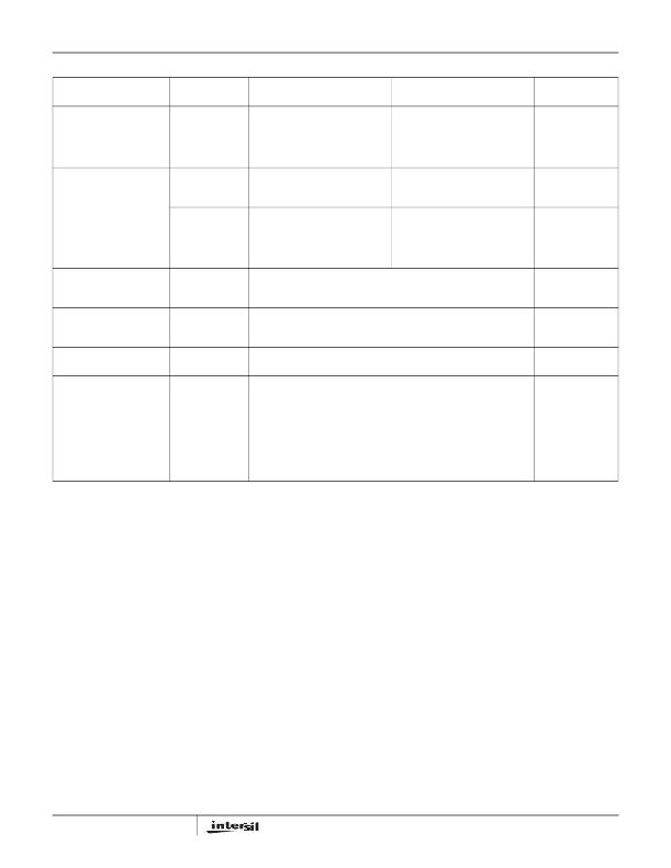
�TABLE� 1.� PROTECTIONS� TABLE� (Continued)�
�DETECTION�
�VOUT�
�CASE�
�6�
�FAILURE� MODE�
�CH0� LED� Open�
�MODE�
�Upper� OTP�
�FAILED� CHANNEL� ACTION�
�CH0� goes� off� until� chip� cooled� and�
�GOOD� CHANNELS� ACTION�
�Same� as� CH0�
�REGULATED� BY�
�VF� of� CH0�
�Circuit� but� has�
�paralleled� Zener�
�triggered� but�
�VIIN0� <� VSC�
�then� comes� back� on� with� current�
�reduced� to� 76%.� Further� OTP�
�triggers� result� in� reduction� to� 53%,�
�then� 30%.�
�7�
�CH0� LED� Open�
�Upper� OTP� not�
�CH0� OFF�
�CH1� through� CH7� Normal�
�Highest� VF� of� CH1�
�Circuit� but� has�
�paralleled� Zener�
�triggered� but�
�VIIN0� >� VSC�
�through� CH7�
�Upper� OTP� not�
�CH0� remains� ON� and� has� highest�
�VOUT� increases� then� CH-X�
�VF� of� CH0�
�triggered� but� VIINx� VF,� thus� VOUT� increases.�
�>� VSC�
�switches� OFF.� This� is� an� unwanted�
�shut� off� and� the� effect� can� be�
�minimized� by� setting� OVP� at� an�
�appropriate� level.�
�8�
�Channel-to-Channel� Lower� OTP�
�Any� channel� at� below� 50%� of� the� target� current� will� fault� out� after� 400μs.�
�Highest� VF� of� CH0�
�Δ� VF� too� high�
�triggered� but� VIINx� Remaining� channels� driven� with� normal� current.�
�<� VSC�
�through� CH7�
�9�
�Channel-to-Channel� Upper� OTP�
�All� channels� switched� off� until� chip� cooled� and� then� comes� back� on� with�
�Highest� VF� of� CH0�
�Δ� VF� too� high�
�triggered� but� VIINx� current� reduced� to� 76%.� Further� OTP� triggers� result� in� reduction� to� 53%,� through� CH7�
�<� VSC�
�then� 30%.�
�10�
�Output� LED� stack�
�voltage� too� high�
�VOUT� >� VOVP�
�Driven� with� normal� current.� Any� channel� that� is� below� 50%� of� the� target�
�current� will� time-out� after� 6ms.�
�Highest� VF� of� CH0�
�through� CH7�
�11�
�VOUT/LX� shorted� to� LX� current� and�
�Fault� switch� disabled� and� system� shutdown� until� fault� goes� away,� VOUT�
�GND�
�timing� are�
�monitored.�
�OVP� pin�
�monitored� for�
�excursions� below�
�20%� of� OVP�
�threshold�
�is� checked� at� start-up� with� a� low� current� from� LX� to� check� for� presence� of�
�short� before� the� fault� switch� is� enabled.�
�Components� Selections�
�According� to� the� inductor� Voltage-Second� Balance� principle,�
�the� change� of� inductor� current� during� the� switching� regulator�
�On� time� is� equal� to� the� change� of� inductor� current� during� the�
�switching� regulator� Off� time.� Since� the� voltage� across� an�
�inductor� is:�
�Input� Capacitor�
�Switching� regulators� require� input� capacitors� to� deliver� peak�
�charging� current� and� to� reduce� the� impedance� of� the� input�
�supply.� This� reduces� interaction� between� the� regulator� and�
�input� supply,� improving� system� stability.� The� high� switching�
�frequency� of� the� loop� causes� almost� all� ripple� current� to� flow�
�in� the� input� capacitor,� which� must� be� rated� accordingly.�
�V� L� =� L� ×� Δ� I� L� ?� Δ� t�
�and� Δ� I� L� @� On� =� Δ� I� L� @� Off,� therefore:�
�(� V� I� –� 0� )� ?� L� ×� D� ×� t� S� =� (� V� O� –� V� D� –� V� I� )� ?� L� ×� (� 1� –� D� )� ×� t� S�
�(EQ.� 5)�
�(EQ.� 6)�
�A� capacitor� with� low� internal� series� resistance� should� be�
�chosen� to� minimize� heating� effects� and� improve� system�
�efficiency,� such� as� X5R� or� X7R� ceramic� capacitors,� which�
�offer� small� size� and� a� lower� value� of� temperature� and� voltage�
�coefficient� compared� to� other� ceramic� capacitors.�
�where� D� is� the� switching� duty� cycle� defined� by� the� turn-on�
�time� over� the� switching� period.� V� D� is� Schottky� diode� forward�
�voltage� that� can� be� neglected� for� approximation.�
�Rearranging� the� terms� without� accounting� for� V� D� gives� the�
�boost� ratio� and� duty� cycle� respectively� as:�
�In� boost� mode,� input� current� flows� continuously� into� the�
�inductor,� with� an� AC� ripple� component� proportional� to� the�
�rate� of� inductor� charging� only� and� smaller� value� input�
�capacitors� may� be� used.� It� is� recommended� that� an� input�
�capacitor� of� at� least� 10μF� be� used.� Ensure� the� voltage� rating�
�of� the� input� capacitor� is� suitable� to� handle� the� full� supply�
�V� O� ?� V� I� =� 1� ?� (� 1� –� D� )�
�(EQ.� 7)�
�range.�
�D� =� (� V� O� –� V� I� )� ?� V� O�
�14�
�(EQ.� 8)�
�FN6570.0�
�May� 9,� 2008�
�相关PDF资料 |
PDF描述 |
|---|---|
| AP431SAG-7 | IC VREF SHUNT PREC ADJ SOT-23-3 |
| RMC44DRXN | CONN EDGECARD 88POS DIP .100 SLD |
| MC7808AEBTG | IC REG LDO 8V 1A TO220AB |
| TPSD337M010H0150 | CAP TANT 330UF 10V 20% 2917 |
| ISL97631IHTZ-T7A | IC LED DRIVR WHITE BCKLGT TSOT-6 |
相关代理商/技术参数 |
参数描述 |
|---|---|
| ISL97636IRZ-TK | 功能描述:IC LED DRIVR WHITE BCKLGT 24-QFN RoHS:是 类别:集成电路 (IC) >> PMIC - LED 驱动器 系列:- 产品培训模块:Lead (SnPb) Finish for COTS Obsolescence Mitigation Program 标准包装:2,500 系列:- 恒定电流:- 恒定电压:- 拓扑:升压(升压),切换式电容器(充电泵) 输出数:1 内部驱动器:是 类型 - 主要:背光 类型 - 次要:白色 LED 频率:625kHz ~ 875kHz 电源电压:2.7 V ~ 5.3 V 输出电压:5V 安装类型:表面贴装 封装/外壳:10-TFSOP,10-MSOP(0.118",3.00mm 宽) 供应商设备封装:10-µMAX 包装:带卷 (TR) 工作温度:-40°C ~ 85°C |
| ISL97642IRTZ | 功能描述:IC REG TFT-LCD DC/DC 32-TQFN RoHS:是 类别:集成电路 (IC) >> PMIC - 电源管理 - 专用 系列:- 应用说明:Ultrasound Imaging Systems Application Note 产品培训模块:Lead (SnPb) Finish for COTS Obsolescence Mitigation Program 标准包装:37 系列:- 应用:医疗用超声波成像,声纳 电流 - 电源:- 电源电压:2.37 V ~ 6 V 工作温度:0°C ~ 70°C 安装类型:表面贴装 封装/外壳:56-WFQFN 裸露焊盘 供应商设备封装:56-TQFN-EP(8x8) 包装:管件 |
| ISL97642IRTZ-T | 功能描述:IC REG TFT-LCD DC/DC 32-TQFN RoHS:是 类别:集成电路 (IC) >> PMIC - 电源管理 - 专用 系列:- 应用说明:Ultrasound Imaging Systems Application Note 产品培训模块:Lead (SnPb) Finish for COTS Obsolescence Mitigation Program 标准包装:37 系列:- 应用:医疗用超声波成像,声纳 电流 - 电源:- 电源电压:2.37 V ~ 6 V 工作温度:0°C ~ 70°C 安装类型:表面贴装 封装/外壳:56-WFQFN 裸露焊盘 供应商设备封装:56-TQFN-EP(8x8) 包装:管件 |
| ISL97642IRTZ-TK | 功能描述:IC REG TFT-LCD DC/DC 32-TQFN RoHS:是 类别:集成电路 (IC) >> PMIC - 电源管理 - 专用 系列:- 应用说明:Ultrasound Imaging Systems Application Note 产品培训模块:Lead (SnPb) Finish for COTS Obsolescence Mitigation Program 标准包装:37 系列:- 应用:医疗用超声波成像,声纳 电流 - 电源:- 电源电压:2.37 V ~ 6 V 工作温度:0°C ~ 70°C 安装类型:表面贴装 封装/外壳:56-WFQFN 裸露焊盘 供应商设备封装:56-TQFN-EP(8x8) 包装:管件 |
| ISL97644IRZ | 制造商:Rochester Electronics LLC 功能描述: 制造商:Intersil Corporation 功能描述: |
发布紧急采购,3分钟左右您将得到回复。