- 您现在的位置:买卖IC网 > PDF目录20671 > ISLUSBI2CKIT1Z (Intersil)KIT ISL6405 PDF资料下载
参数资料
| 型号: | ISLUSBI2CKIT1Z |
| 厂商: | Intersil |
| 文件页数: | 8/13页 |
| 文件大小: | 0K |
| 描述: | KIT ISL6405 |
| 标准包装: | 1 |
| 系列: | * |
�� �
�
�ISL6405�
�This� feature� only� affects� the� turn-on� and� programmed�
�TABLE� 1.�
�voltage� rise� and� fall� times.�
�Current� Limiting�
�The� current� limiting� block� has� two� thresholds� that� can� be�
�selected� by� the� ISEL� bit� of� the� SR� and� can� work� either�
�statically� (simple� current� clamp)� or� dynamically.� The� lower�
�threshold� is� between� 425mA� and� 530mA� (ISEL� =� L),� while�
�I� 2� C� BITS�
�13V�
�14V�
�13V�
�14V�
�SEL18V� (1,� 2)�
�Low�
�Low�
�High�
�High�
�O/P� VOLTAGE�
�13V�
�14V�
�18V�
�19V�
�the� higher� threshold� is� between� 775mA� and� 925mA�
�(ISEL� =� H).� When� the� DCL� (Dynamic� Current� Limiting)� bit� is�
�set� to� LOW,� the� over� current� protection� circuit� works�
�dynamically:� as� soon� as� an� overload� is� detected,� the� output�
�is� shutdown� for� a� time� t� OFF� ,� typically� 900ms.� Simultaneously�
�the� OLF� bit� of� the� System� Register� is� set� to� HIGH.� After� this�
�time� has� elapsed,� the� output� is� resumed� for� a� time� t� ON� =�
�20ms.� During� t� ON� ,� the� device� output� will� be� current� limited� to�
�425mA� or� 775mA,� depending� on� the� ISEL� bits.� At� the� end� of�
�t� ON� ,� if� the� overload� is� still� detected,� the� protection� circuit� will�
�cycle� again� through� t� OFF� and� t� ON� .� At� the� end� of� a� full� t� ON� in�
�which� no� overload� is� detected,� normal� operation� is� resumed�
�and� the� OLF� bit� is� reset� to� LOW.� Typical� t� ON� +� t� OFF� time� is�
�920ms� as� determined� by� an� internal� timer.� This� dynamic�
�operation� can� greatly� reduce� the� power� dissipation� in� a� short�
�circuit� condition,� still� ensuring� excellent� power-on� start-up� in�
�most� conditions.�
�However,� there� could� be� some� cases� in� which� a� highly�
�capacitive� load� on� the� output� may� cause� a� difficult� start-up�
�when� the� dynamic� protection� is� chosen.� This� can� be� solved�
�by� initiating� any� power� start-up� in� static� mode� (DCL� =� HIGH)�
�and� then� switching� to� the� dynamic� mode� (DCL� =� LOW)� after�
�a� chosen� amount� of� time.� When� in� static� mode,� the� OLF1/2�
�bit� goes� HIGH� when� the� current� clamp� limit� is� reached� and�
�returns� LOW� when� the� overload� condition� is� cleared.� The�
�OLF1/2� bit� will� be� LOW� at� the� end� of� initial� power-on� soft-start.�
�Thermal� Protection�
�I� 2� C� Bus� Interface� for� ISL6405�
�(Refer� to� Philips� I� 2� C� Specification,� Rev.� 2.1)�
�Data� transmission� from� main� microprocessor� to� the� ISL6405�
�and� vice� versa� takes� place� through� the� two� wire� I� 2� C� bus�
�interface,� consisting� of� the� two� lines� SDA� and� SCL.� Both� SDA�
�and� SCL� are� bidirectional� lines,� connected� to� a� positive� supply�
�voltage� via� a� pull� up� resistor.� (Pull� up� resistors� to� positive� supply�
�voltage� must� be� externally� connected).� When� the� bus� is� free,�
�both� lines� are� HIGH.� The� output� stages� of� ISL6405� will� have� an�
�open� drain/open� collector� in� order� to� perform� the� wired-AND�
�function.� Data� on� the� I� 2� C� bus� can� be� transferred� up� to� 100Kbps�
�in� the� standard-mode� or� up� to� 400Kbps� in� the� fast-mode.� The�
�level� of� logic� “0”� and� logic� “1”� is� dependent� of� associated� value�
�of� V� DD� as� per� electrical� specification� table.� One� clock� pulse� is�
�generated� for� each� data� bit� transferred.�
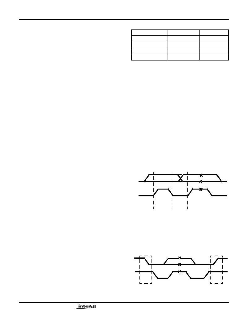
�Data� Validity�
�The� data� on� the� SDA� line� must� be� stable� during� the� HIGH�
�period� of� the� clock.� The� HIGH� or� LOW� state� of� the� data� line�
�can� only� change� when� the� clock� signal� on� the� SCL� line� is�
�LOW.� Refer� to� Figure� 1.�
�SDA�
�SCL�
�This� IC� is� protected� against� overheating.� When� the� junction�
�DATA� LINE�
�STABLE�
�CHANGE�
�OF� DATA�
�temperature� exceeds� 150°C� (typical),� the� step-up� converter�
�and� the� linear� regulator� are� shut� off� and� the� OTF� bit� of� the�
�SR� is� set� HIGH.� Normal� operation� is� resumed� and� the� OTF�
�bit� is� reset� LOW� when� the� junction� is� cooled� down� to� 135°C�
�(typical).�
�In� over� temperature� conditions,� the� OTF� Flag� goes� HIGH�
�and� the� I� 2� C� data� will� be� cleared.� The� user� may� need� to�
�monitor� the� I� 2� C� enable� bits� and� OTF� flag� continuously� and�
�enable� the� chip,� if� I� 2� C� data� is� cleared.� OTF� conditions� may�
�also� make� the� OLF� flags� go� HIGH,� when� high� capacitive�
�loads� are� present� or� self-heating� conditions� occur� at� higher�
�loads.�
�External� Output� Voltage� Selection�
�The� output� voltage� can� be� selected� by� the� I� 2� C� bus.�
�DATA� VALID� ALLOWED�
�FIGURE� 1.� DATA� VALIDITY�
�START� and� STOP� Conditions�
�As� shown� in� Figure� 2,� START� condition� is� a� HIGH� to� LOW�
�transition� of� the� SDA� line� while� SCL� is� HIGH.�
�The� STOP� condition� is� a� LOW� to� HIGH� transition� on� the� SDA�
�line� while� SCL� is� HIGH.� A� STOP� condition� must� be� sent�
�before� each� START� condition.�
�SDA�
�SCL�
�Additionally,� the� QFN� package� offers� two� pins� (SEL18V1,�
�SEL18V2)� for� independent� 13V/18V� output� voltage�
�selection.� When� using� these� pins,� the� I� 2� C� bits� should� be�
�S�
�START�
�CONDITION�
�P�
�STOP�
�CONDITION�
�initialized� to� 13V� status.�
�8�
�FIGURE� 2.� START� AND� STOP� WAVEFORMS�
�相关PDF资料 |
PDF描述 |
|---|---|
| ISL6207HRZ-T | IC MOSFET DRVR SYNC BUCK 8-QFN |
| B160-E3/61T | DIODE SCHOTTKY 1A 60V SMA |
| VE-2NL-EW-B1 | CONVERTER MOD DC/DC 28V 100W |
| EMC43DRAN | CONN EDGECARD 86POS R/A .100 SLD |
| ECM08DRPS | CONN EDGECARD 16POS DIP .156 SLD |
相关代理商/技术参数 |
参数描述 |
|---|---|
| ISM001DR09L-70 | 制造商:未知厂家 制造商全称:未知厂家 功能描述:x(8+1) Fast Page Mode DRAM Module |
| ISM001DR09L-80 | 制造商:未知厂家 制造商全称:未知厂家 功能描述:x(8+1) Fast Page Mode DRAM Module |
| ISM001DR09P-70 | 制造商:未知厂家 制造商全称:未知厂家 功能描述:x(8+1) Fast Page Mode DRAM Module |
| ISM001DR09P-80 | 制造商:未知厂家 制造商全称:未知厂家 功能描述:x(8+1) Fast Page Mode DRAM Module |
| ISM001FLKA-120 | 制造商:未知厂家 制造商全称:未知厂家 功能描述:x16 Flash EEPROM Module |
发布紧急采购,3分钟左右您将得到回复。