- 您现在的位置:买卖IC网 > PDF目录19740 > ISPLSI 2096A-125LQN128 (Lattice Semiconductor Corporation)IC PLD ISP 96I/O 7.5NS 128PQFP PDF资料下载
参数资料
| 型号: | ISPLSI 2096A-125LQN128 |
| 厂商: | Lattice Semiconductor Corporation |
| 文件页数: | 1/12页 |
| 文件大小: | 0K |
| 描述: | IC PLD ISP 96I/O 7.5NS 128PQFP |
| 标准包装: | 24 |
| 系列: | ispLSI® 2000A |
| 可编程类型: | 系统内可编程 |
| 最大延迟时间 tpd(1): | 7.5ns |
| 电压电源 - 内部: | 4.75 V ~ 5.25 V |
| 逻辑元件/逻辑块数目: | 24 |
| 宏单元数: | 96 |
| 门数: | 4000 |
| 输入/输出数: | 96 |
| 工作温度: | 0°C ~ 70°C |
| 安装类型: | 表面贴装 |
| 封装/外壳: | 128-BQFP |
| 供应商设备封装: | 128-PQFP(28x28) |
| 包装: | 托盘 |
| 其它名称: | ISPLSI2096A-125LQN128 |
ispLSI
2096/A
In-System Programmable High Density PLD
2096_09
1
USE
ispLSI
2096E
FOR
NEW
DESIGNS
Lead-
Free
Package
Options
Available!
Features
ENHANCEMENTS
— ispLSI 2096A is Fully Form and Function Compatible
to the ispLSI 2096, with Identical Timing
Specifcations and Packaging
— ispLSI 2096A is Built on an Advanced 0.35 Micron
E2CMOS Technology
HIGH DENSITY PROGRAMMABLE LOGIC
— 4000 PLD Gates
— 96 I/O Pins, Six Dedicated Inputs
— 96 Registers
— High Speed Global Interconnect
— Wide Input Gating for Fast Counters, State
Machines, Address Decoders, etc.
— Small Logic Block Size for Random Logic
HIGH PERFORMANCE E2CMOS TECHNOLOGY
—
fmax = 125 MHz Maximum Operating Frequency
—
tpd = 7.5 ns Propagation Delay
— TTL Compatible Inputs and Outputs
— Electrically Erasable and Reprogrammable
— Non-Volatile
— 100% Tested at Time of Manufacture
— Unused Product Term Shutdown Saves Power
IN-SYSTEM PROGRAMMABLE
— In-System Programmable (ISP) 5V Only
— Increased Manufacturing Yields, Reduced Time-to-
Market and Improved Product Quality
— Reprogram Soldered Devices for Faster Prototyping
OFFERS THE EASE OF USE AND FAST SYSTEM
SPEED OF PLDs WITH THE DENSITY AND FLEXIBILITY
OF FIELD PROGRAMMABLE GATE ARRAYS
— Complete Programmable Device Can Combine
Glue Logic and Structured Designs
— Enhanced Pin Locking Capability
— Three Dedicated Clock Input Pins
— Synchronous and Asynchronous Clocks
— Programmable Output Slew Rate Control to
Minimize Switching Noise
— Flexible Pin Placement
— Optimized Global Routing Pool Provides Global
Interconnectivity
— Lead-Free Package Options
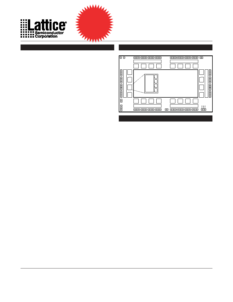
Functional Block Diagram
Global Routing Pool
(GRP)
Output Routing Pool (ORP)
0919/2096
C7
C4
C5
C6
A4
A7
A6
A5
GLB
Logic
Array
DQ
Output Routing Pool (ORP)
C3
C0
C1
C2
B0
B3
B2
B1
Output
Routing
Pool
(ORP)
Output
Routing
Pool
(ORP)
B7
B6
B4
B5
A0
A1
A3
A2
Description
The ispLSI 2096 and 2096A are High Density Program-
mable Logic Devices. The devices contain 96 Registers,
96 Universal I/O pins, six Dedicated Input pins, three
Dedicated Clock Input pins, two dedicated Global OE
input pins and a Global Routing Pool (GRP). The GRP
provides complete interconnectivity between all of these
elements. The ispLSI 2096 and 2096A feature 5V in-
system programmability and in-system diagnostic
capabilities. The ispLSI 2096 and 2096A offer non-
volatile reprogrammability of the logic, as well as the
interconnect to provide truly reconfigurable systems.
The basic unit of logic on these devices is the Generic
Logic Block (GLB). The GLBs are labeled A0, A1…C7
(Figure 1). There are a total of 24 GLBs in the ispLSI 2096
and 2096A devices. Each GLB is made up of four
macrocells. Each GLB has 18 inputs, a programmable
AND/OR/Exclusive OR array, and four outputs which can
be configured to be either combinatorial or registered.
Inputs to the GLB come from the GRP and dedicated
inputs. All of the GLB outputs are brought back into the
GRP so that they can be connected to the inputs of any
GLB on the device.
Copyright 2006 Lattice Semiconductor Corp. All brand or product names are trademarks or registered trademarks of their respective holders. The specifications and information herein are subject
to change without notice.
LATTICE SEMICONDUCTOR CORP., 5555 Northeast Moore Ct., Hillsboro, Oregon 97124, U.S.A.
Tel. (503) 268-8000; 1-800-LATTICE; FAX (503) 268-8556; http://www.latticesemi.com
August 2006
Select
devices
have
been
discontinued.
See
Ordering
Information
section
for
product
status.
相关PDF资料 |
PDF描述 |
|---|---|
| VI-26T-EV-F4 | CONVERTER MOD DC/DC 6.5V 150W |
| VI-B5Y-CX-F2 | CONVERTER MOD DC/DC 3.3V 49.5W |
| VI-26T-EV-F3 | CONVERTER MOD DC/DC 6.5V 150W |
| VI-B5Y-CW-F4 | CONVERTER MOD DC/DC 3.3V 66W |
| VI-B5Y-CW-F3 | CONVERTER MOD DC/DC 3.3V 66W |
相关代理商/技术参数 |
参数描述 |
|---|---|
| ispLSI2096A-125LQN128 | 功能描述:CPLD - 复杂可编程逻辑器件 USE ispMACH 4000V RoHS:否 制造商:Lattice 系列: 存储类型:EEPROM 大电池数量:128 最大工作频率:333 MHz 延迟时间:2.7 ns 可编程输入/输出端数量:64 工作电源电压:3.3 V 最大工作温度:+ 90 C 最小工作温度:0 C 封装 / 箱体:TQFP-100 |
| ispLSI2096A-125LT128 | 功能描述:CPLD - 复杂可编程逻辑器件 USE ispMACH 4000V RoHS:否 制造商:Lattice 系列: 存储类型:EEPROM 大电池数量:128 最大工作频率:333 MHz 延迟时间:2.7 ns 可编程输入/输出端数量:64 工作电源电压:3.3 V 最大工作温度:+ 90 C 最小工作温度:0 C 封装 / 箱体:TQFP-100 |
| ispLSI2096A-125LTN128 | 功能描述:CPLD - 复杂可编程逻辑器件 USE ispMACH 4000V RoHS:否 制造商:Lattice 系列: 存储类型:EEPROM 大电池数量:128 最大工作频率:333 MHz 延迟时间:2.7 ns 可编程输入/输出端数量:64 工作电源电压:3.3 V 最大工作温度:+ 90 C 最小工作温度:0 C 封装 / 箱体:TQFP-100 |
| ispLSI2096A-80LQ128 | 功能描述:CPLD - 复杂可编程逻辑器件 USE ispMACH 4000V RoHS:否 制造商:Lattice 系列: 存储类型:EEPROM 大电池数量:128 最大工作频率:333 MHz 延迟时间:2.7 ns 可编程输入/输出端数量:64 工作电源电压:3.3 V 最大工作温度:+ 90 C 最小工作温度:0 C 封装 / 箱体:TQFP-100 |
| ispLSI2096A-80LQ128I | 功能描述:CPLD - 复杂可编程逻辑器件 USE ispMACH 4000V RoHS:否 制造商:Lattice 系列: 存储类型:EEPROM 大电池数量:128 最大工作频率:333 MHz 延迟时间:2.7 ns 可编程输入/输出端数量:64 工作电源电压:3.3 V 最大工作温度:+ 90 C 最小工作温度:0 C 封装 / 箱体:TQFP-100 |
发布紧急采购,3分钟左右您将得到回复。