- 您现在的位置:买卖IC网 > PDF目录19593 > ISPLSI 5384VA-125LB272 (Lattice Semiconductor Corporation)IC PLD ISP 288I/O 7.5NS 272BGA PDF资料下载
参数资料
| 型号: | ISPLSI 5384VA-125LB272 |
| 厂商: | Lattice Semiconductor Corporation |
| 文件页数: | 9/31页 |
| 文件大小: | 0K |
| 描述: | IC PLD ISP 288I/O 7.5NS 272BGA |
| 标准包装: | 40 |
| 系列: | ispLSI® 5000VA |
| 可编程类型: | 系统内可编程 |
| 最大延迟时间 tpd(1): | 7.5ns |
| 电压电源 - 内部: | 3 V ~ 3.6 V |
| 逻辑元件/逻辑块数目: | 12 |
| 宏单元数: | 384 |
| 门数: | 18000 |
| 输入/输出数: | 192 |
| 工作温度: | 0°C ~ 70°C |
| 安装类型: | 表面贴装 |
| 封装/外壳: | 272-BBGA |
| 供应商设备封装: | 272-BGA(27x27) |
| 包装: | 托盘 |
| 其它名称: | ISPLSI5384VA-125LB272 |
第1页第2页第3页第4页第5页第6页第7页第8页当前第9页第10页第11页第12页第13页第14页第15页第16页第17页第18页第19页第20页第21页第22页第23页第24页第25页第26页第27页第28页第29页第30页第31页
Specifications ispLSI 5384VA
17
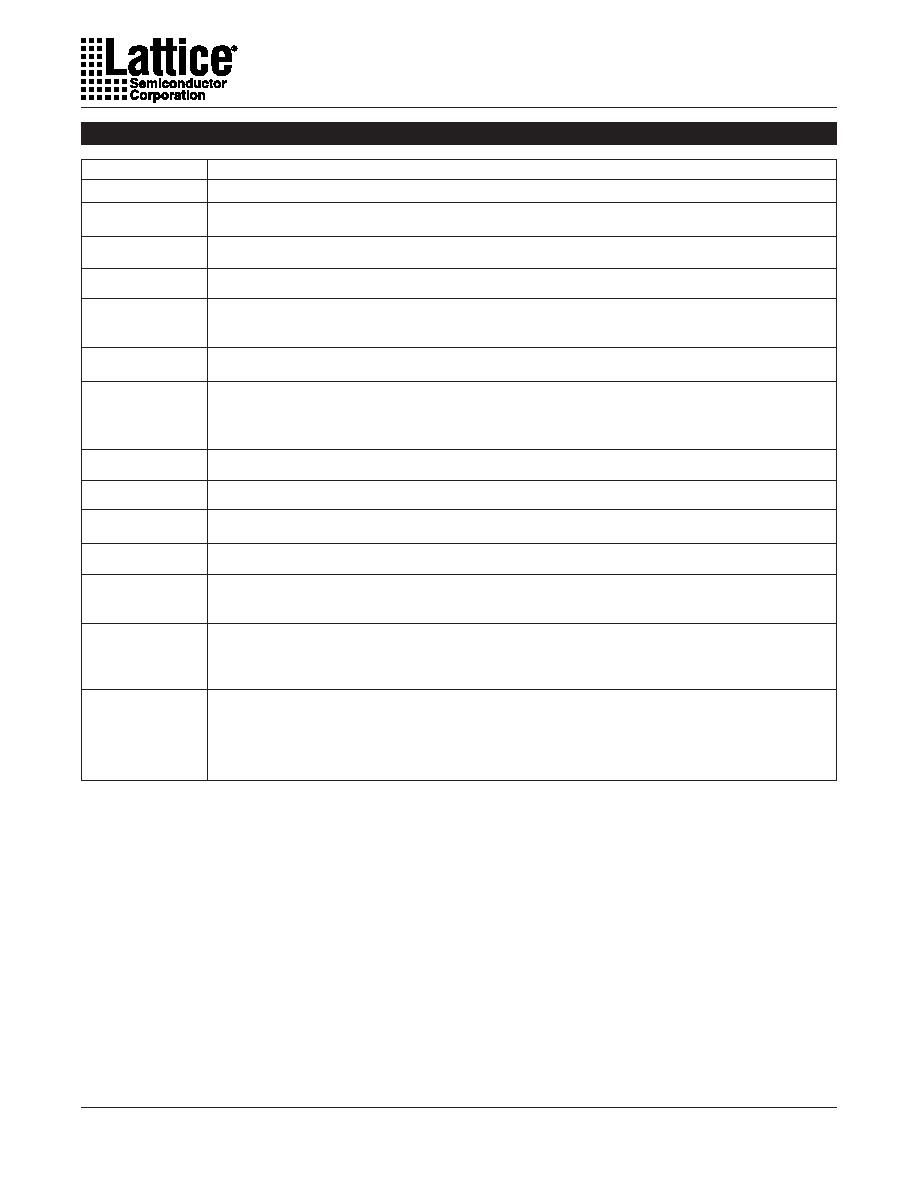
TMS
Input - This pin is the Test Mode Select input, which is used to control the JTAG state machine.
TCK
Input - This pin is the Test Clock input pin used to clock through the JTAG state machine.
TDI
Input - This pin is the JTAG Test Data In pin used to load data.
TDO
Output - This pin is the JTAG Test Data Out pin used to shift data out.
TOE / I/O0
Input/Output - This pin functions as either the Test Output Enable pin or an I/O pin based upon
customer's design. TOE tristates all I/O pins when a logic low is driven.
GOE0, GOE1
Input - These two pins are the Global Output Enable input pins.
GSET/GRST
Dedicated Set/Reset Input - This pin is available to all registers in the device and can
independently be configured as preset, reset or no effect on each register. The global polarity
(active high or low input) for this pin is also selectable.
I/O
Input/Output – These are the general purpose I/O used by the logic array.
GND
Ground
NC1
No connect.
VCC
Vcc
CLK0, CLK1
Dedicated clock inputs for all registers. Both clocks are muxed before being used as the clock
input to all registers in the device.
CLK2 / I/O,
Input/Output - These pins function as either dedicated clock inputs for all registers or an I/O
CLK3 / I/O
pin based upon customer's design. Both clocks are muxed before being used as the clock input
to all registers in the device.
VCCIO
Input - This pin is used if an optional 2.5V output is to be used. Every IO can independently
select either 3.3V or the optional voltage as its output level. If the optional output voltage is
not required, this pin must be connected to the Vcc supply. Programmable pull-up resistors and
bus-hold latches only draw current from this supply.
Signal Descriptions
Signal Name
Description
1. NC pins are not to be connected to any active signals, VCC or GND.
相关PDF资料 |
PDF描述 |
|---|---|
| GCM10DTMD-S189 | CONN EDGECARD 20POS R/A .156 SLD |
| EPM7032SLC44-7 | IC MAX 7000 CPLD 32 44-PLCC |
| MAX6698EE99+ | IC TEMP MONITOR 7CH 16-QSOP |
| GEC07DRTH-S13 | CONN EDGECARD 14POS .100 EXTEND |
| VI-2TZ-CX-F1 | CONVERTER MOD DC/DC 2V 30W |
相关代理商/技术参数 |
参数描述 |
|---|---|
| ISPLSI5384VA-125LB272 | 功能描述:CPLD - 复杂可编程逻辑器件 RoHS:否 制造商:Lattice 系列: 存储类型:EEPROM 大电池数量:128 最大工作频率:333 MHz 延迟时间:2.7 ns 可编程输入/输出端数量:64 工作电源电压:3.3 V 最大工作温度:+ 90 C 最小工作温度:0 C 封装 / 箱体:TQFP-100 |
| ISPLSI5384VA-125LB388 | 功能描述:CPLD - 复杂可编程逻辑器件 RoHS:否 制造商:Lattice 系列: 存储类型:EEPROM 大电池数量:128 最大工作频率:333 MHz 延迟时间:2.7 ns 可编程输入/输出端数量:64 工作电源电压:3.3 V 最大工作温度:+ 90 C 最小工作温度:0 C 封装 / 箱体:TQFP-100 |
| ISPLSI5384VA-125LQ208 | 功能描述:CPLD - 复杂可编程逻辑器件 RoHS:否 制造商:Lattice 系列: 存储类型:EEPROM 大电池数量:128 最大工作频率:333 MHz 延迟时间:2.7 ns 可编程输入/输出端数量:64 工作电源电压:3.3 V 最大工作温度:+ 90 C 最小工作温度:0 C 封装 / 箱体:TQFP-100 |
| ISPLSI5384VA-70LB208 | 功能描述:CPLD - 复杂可编程逻辑器件 RoHS:否 制造商:Lattice 系列: 存储类型:EEPROM 大电池数量:128 最大工作频率:333 MHz 延迟时间:2.7 ns 可编程输入/输出端数量:64 工作电源电压:3.3 V 最大工作温度:+ 90 C 最小工作温度:0 C 封装 / 箱体:TQFP-100 |
| ISPLSI5384VA-70LB272 | 功能描述:CPLD - 复杂可编程逻辑器件 RoHS:否 制造商:Lattice 系列: 存储类型:EEPROM 大电池数量:128 最大工作频率:333 MHz 延迟时间:2.7 ns 可编程输入/输出端数量:64 工作电源电压:3.3 V 最大工作温度:+ 90 C 最小工作温度:0 C 封装 / 箱体:TQFP-100 |
发布紧急采购,3分钟左右您将得到回复。