- 您现在的位置:买卖IC网 > PDF目录19631 > ISPLSI 5384VA-70LB272I (Lattice Semiconductor Corporation)IC PLD ISP 288I/O 15NS 272BGA PDF资料下载
参数资料
| 型号: | ISPLSI 5384VA-70LB272I |
| 厂商: | Lattice Semiconductor Corporation |
| 文件页数: | 1/31页 |
| 文件大小: | 0K |
| 描述: | IC PLD ISP 288I/O 15NS 272BGA |
| 标准包装: | 40 |
| 系列: | ispLSI® 5000VA |
| 可编程类型: | 系统内可编程 |
| 最大延迟时间 tpd(1): | 15.0ns |
| 电压电源 - 内部: | 3 V ~ 3.6 V |
| 逻辑元件/逻辑块数目: | 12 |
| 宏单元数: | 384 |
| 门数: | 18000 |
| 输入/输出数: | 192 |
| 工作温度: | -40°C ~ 85°C |
| 安装类型: | 表面贴装 |
| 封装/外壳: | 272-BBGA |
| 供应商设备封装: | 272-BGA(27x27) |
| 包装: | 托盘 |
| 其它名称: | ISPLSI5384VA-70LB272I |
当前第1页第2页第3页第4页第5页第6页第7页第8页第9页第10页第11页第12页第13页第14页第15页第16页第17页第18页第19页第20页第21页第22页第23页第24页第25页第26页第27页第28页第29页第30页第31页
ispLSI 5384VA
In-System Programmable
3.3V SuperWIDE High Density PLD
1
5384va_08
Copyright 2002 Lattice Semiconductor Corp. All brand or product names are trademarks or registered trademarks of their respective holders. The specifications and information herein are subject
to change without notice.
LATTICE SEMICONDUCTOR CORP., 5555 Northeast Moore Ct., Hillsboro, Oregon 97124, U.S.A.
January 2002
Tel. (503) 268-8000; 1-800-LATTICE; FAX (503) 268-8556; http://www.latticesemi.com
Features
SuperWIDE HIGH-DENSITY IN-SYSTEM
PROGRAMMABLE LOGIC
— 3.3V Power Supply
— User Selectable 3.3V/2.5V I/O
— 18,000 PLD Gates / 384 Macrocells
— Up to 288 I/O Pins
— 384 Registers
— High-Speed Global Interconnect
— SuperWIDE 32 Generic Logic Block (GLB) Size for
Optimum Performance
— SuperWIDE Input Gating (68 Inputs) for Fast
Counters, State Machines, Address Decoders, etc.
— PCB Efficient Ball Grid Array (BGA) Package Options
— Interfaces with Standard 5V TTL Devices
HIGH PERFORMANCE E2CMOS TECHNOLOGY
—
fmax = 125 MHz Maximum Operating Frequency
—
tpd = 7.5 ns Propagation Delay
— Enhanced
tsu2 = 7 ns, tsu3 (CLK0/1) = 4.5ns,
tsu3 (CLK2/3) = 3.5ns
— TTL/3.3V/2.5V Compatible Input Thresholds and
Output Levels
— Electrically Erasable and Reprogrammable
— Non-Volatile
— Programmable Speed/Power Logic Path Optimization
IN-SYSTEM PROGRAMMABLE
— Increased Manufacturing Yields, Reduced Time-to-
Market, and Improved Product Quality
— Reprogram Soldered Devices for Faster Debugging
100% IEEE 1149.1 BOUNDARY SCAN TESTABLE AND
3.3V IN-SYSTEM PROGRAMMABLE
ARCHITECTURE FEATURES
— Enhanced Pin-Locking Architecture with Single-
Level Global Routing Pool and SuperWIDE GLBs
— Wrap Around Product Term Sharing Array Supports
up to 35 Product Terms Per Macrocell
— Macrocells Support Concurrent Combinatorial and
Registered Functions
— Macrocell Registers Feature Multiple Control
Options Including Set, Reset and Clock Enable
— Four Dedicated Clock Input Pins Plus Macrocell
Product Term Clocks
— Slew and Skew Programmable I/O (SASPI/O)
Supports Programmable Bus Hold, Pull-up, Open
Drain and Slew and Skew Rate Options
— Six Global Output Enable Terms, Two Global OE
Pins and One Product Term OE per Macrocell
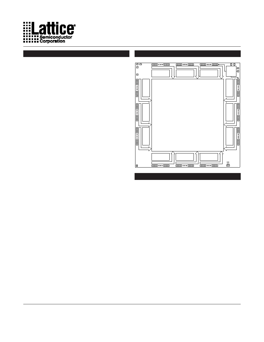
Functional Block Diagram
Global Routing Pool
(GRP)
Boundary
Scan
Interface
Input Bus
Generic
Logic Block
Input Bus
Generic
Logic Block
Input Bus
Generic
Logic Block
Generic
Logic Block
Generic
Logic Block
Generic
Logic Block
Input
Bus
Generic
Logic
Block
Input
Bus
Generic
Logic
Block
Input
Bus
Input
Bus
Input
Bus
Input
Bus
Generic
Logic
Block
Generic
Logic
Block
Generic
Logic
Block
Generic
Logic
Block
ispLSI 5000V Description
The ispLSI 5000V Family of In-System Programmable
High Density Logic Devices is based on Generic Logic
Blocks (GLBs) of 32 registered macrocells and a single
Global Routing Pool (GRP) structure interconnecting the
GLBs.
Outputs from the GLBs drive the Global Routing Pool
(GRP) between the GLBs. Switching resources are pro-
vided to allow signals in the Global Routing Pool to drive
any or all the GLBs in the device. This mechanism allows
fast, efficient connections across the entire device.
Each GLB contains 32 macrocells and a fully populated,
programmable AND-array with 160 logic product terms
and five extra control product terms. The GLB has 68
inputs from the Global Routing Pool which are available
in both true and complement form for every product term.
The 160 product terms are grouped in 32 sets of five and
sent into a Product Term Sharing Array (PTSA) which
allows sharing up to a maximum of 35 product terms for
a single function. Alternatively, the PTSA can be by-
passed for functions of five product terms or less. The
相关PDF资料 |
PDF描述 |
|---|---|
| VE-BWH-CW-B1 | CONVERTER MOD DC/DC 52V 100W |
| PQ015EH02ZZH | IC REG LDO 1.5V 2A TO-263 |
| VE-BTZ-CW-F4 | CONVERTER MOD DC/DC 2V 40W |
| RMA32DTBT | CONN EDGECARD 64POS R/A .125 SLD |
| HWS50-15/HD | PWR SUP IND 15V 52.5W 3.5A |
相关代理商/技术参数 |
参数描述 |
|---|---|
| ISPLSI5384VA-70LB272I | 功能描述:CPLD - 复杂可编程逻辑器件 RoHS:否 制造商:Lattice 系列: 存储类型:EEPROM 大电池数量:128 最大工作频率:333 MHz 延迟时间:2.7 ns 可编程输入/输出端数量:64 工作电源电压:3.3 V 最大工作温度:+ 90 C 最小工作温度:0 C 封装 / 箱体:TQFP-100 |
| ISPLSI5384VA-70LB388 | 功能描述:CPLD - 复杂可编程逻辑器件 RoHS:否 制造商:Lattice 系列: 存储类型:EEPROM 大电池数量:128 最大工作频率:333 MHz 延迟时间:2.7 ns 可编程输入/输出端数量:64 工作电源电压:3.3 V 最大工作温度:+ 90 C 最小工作温度:0 C 封装 / 箱体:TQFP-100 |
| ISPLSI5384VA-70LB388I | 制造商:Lattice Semiconductor Corporation 功能描述: |
| ISPLSI5384VA-70LQ208 | 功能描述:CPLD - 复杂可编程逻辑器件 RoHS:否 制造商:Lattice 系列: 存储类型:EEPROM 大电池数量:128 最大工作频率:333 MHz 延迟时间:2.7 ns 可编程输入/输出端数量:64 工作电源电压:3.3 V 最大工作温度:+ 90 C 最小工作温度:0 C 封装 / 箱体:TQFP-100 |
| ISPLSI5384VE-100LB272 | 功能描述:CPLD - 复杂可编程逻辑器件 RoHS:否 制造商:Lattice 系列: 存储类型:EEPROM 大电池数量:128 最大工作频率:333 MHz 延迟时间:2.7 ns 可编程输入/输出端数量:64 工作电源电压:3.3 V 最大工作温度:+ 90 C 最小工作温度:0 C 封装 / 箱体:TQFP-100 |
发布紧急采购,3分钟左右您将得到回复。