- 您现在的位置:买卖IC网 > PDF目录378642 > IT1750 (CALOGIC LLC) N-Channel Enhancement Mode MOSFET General Purpose Amplifier Switch PDF资料下载
参数资料
| 型号: | IT1750 |
| 厂商: | CALOGIC LLC |
| 元件分类: | 小信号晶体管 |
| 英文描述: | N-Channel Enhancement Mode MOSFET General Purpose Amplifier Switch |
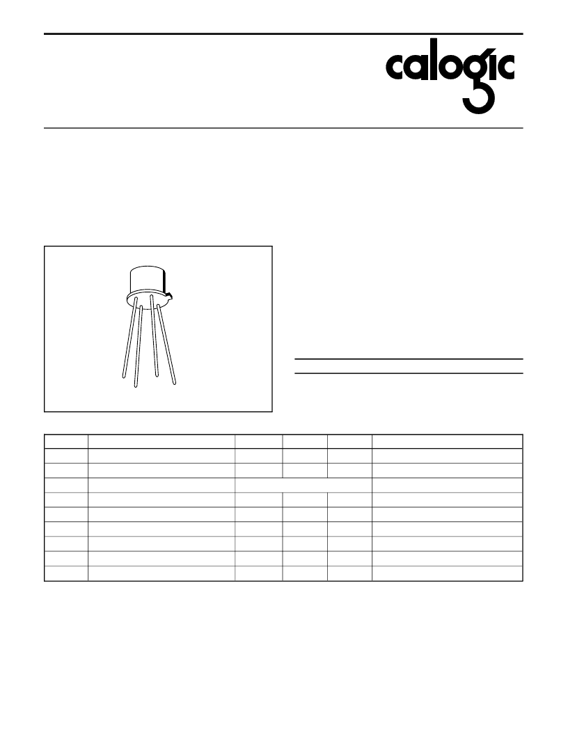
| 中文描述: | 100 mA, 25 V, N-CHANNEL, Si, SMALL SIGNAL, MOSFET, TO-72 |
| 文件页数: | 1/1页 |
| 文件大小: | 17K |
| 代理商: | IT1750 |
N-Channel
Enhancement Mode MOSFET
General Purpose Ampifier Switch
IT1750
FEATURES
Low ON Resistance
Low C
dg
High Gain
Low Threshold Voltage
ABSOLUTE MAXIMUM RATINGS
(T
A
= 25
o
C unless otherwise specified)
Drain-Source and Gate-Source Voltage . . . . . . . . . . . . . . 25V
Peak Gate-Source Voltage (Note 1) . . . . . . . . . . . . . . .
±
125V
Drain Current . . . . . . . . . . . . . . . . . . . . . . . . . . . . . . . . 100mA
Storage Temperature Range . . . . . . . . . . . . . -65
o
C to +200
o
C
Operating Temperature Range . . . . . . . . . . . -65
o
C to +150
o
C
Lead Temperature (Soldering, 10sec). . . . . . . . . . . . . +300
o
C
Power Dissipation . . . . . . . . . . . . . . . . . . . . . . . . . . . . 375mW
Derate above 25
o
C . . . . . . . . . . . . . . . . . . . . . . . . 3mW/
o
C
NOTE:
Stresses above those listed under "Absolute Maximum
Ratings" may cause permanent damage to the device. These are
stress ratings only and functional operation of the device at these or
any other conditions above those indicated in the operational sections
of the specifications is not implied. Exposure to absolute maximum
rating conditions for extended periods may affect device reliability.
ORDERING INFORMATION
Part
IT1750
XIT1750
Package
Hermetic TO-72
Sorted Chips in Carriers
Temperature Range
-55
o
C to +150
o
C
-55
o
C to +150
o
C
C ORPORATION
PIN CONFIGURATION
TO-72
G
D
C
S
1003
ELECTRICAL CHARACTERISTICS
(T
A
= 25
o
C, Body connected to Source and V
BS
= 0 unless otherwise specified)
SYMBOL
PARAMETER
MIN
MAX
UNITS
TEST CONDITIONS
V
GS(th)
Gate to Source Threshold Voltage
0.50
3.0
V
V
DS
= V
GS
, I
D
= 10
μ
A
I
DSS
Drain Leakage Current
10
nA
V
DS
= 10V, V
GS
= 0
I
GSS
Gate Leakage Current
(See note 2)
BV
DSS
Drain Breakdown Voltage
25
V
I
D
= 10
μ
A, V
GS
= 0
r
DS(on)
Drain to Source on Resistance
50
ohms
V
GS
= 20V
I
D(on)
Drain Current
10
mA
V
DS
= V
GS
=10V
Y
fs
Forward Transadmittance
3,000
μ
S
V
DS
= 10V, I
D
= 10mA, f = 1kHz
C
iss
Total Gate Input Capacitance
6.0
pF
I
D
= 10mA, V
DS
= 10V, f = 1MHz (Note 3)
C
dg
Gate to Drain Capacitance
1.6
pF
V
DG
= 10V, f = 1MHz (Note 3)
NOTES: 1.
Devices must not be tested at
±
125V more than once nor longer than 300ms.
2.
Actual gate current is immeasurable. Package suppliers are required to guarantee a package leakage of < 10pA.
External package leakage is the dominant mode which is sensitive to both transient and storage environment, which cannot be guaranteed.
3.
For design reference only, not 100% tested.
相关PDF资料 |
PDF描述 |
|---|---|
| ITH08F06 | HIGH - SPEED POWERLINE N - CHANNEL IGBT |
| IW4001B | Quad 2-Input NOR Gate High-Voltage Silicon-Gate CMOS |
| IW4001BD | Quad 2-Input NOR Gate High-Voltage Silicon-Gate CMOS |
| IW4001BN | Quad 2-Input NOR Gate High-Voltage Silicon-Gate CMOS |
| IW4013B | Dual D Flip-Flop High-Voltage Silicon-Gate CMOS |
相关代理商/技术参数 |
参数描述 |
|---|---|
| IT18 | 制造商:未知厂家 制造商全称:未知厂家 功能描述:ISOTAB TRIACS ELECTRICALLY ISOLATED |
| IT18/3 | 制造商:INSULATED TOOLS 功能描述:SCREWDRIVER 1000V SLOT 3X75MM |
| IT18/4 | 制造商:INSULATED TOOLS 功能描述:SCREWDRIVER 1000V SLOT 3X100MM 制造商:INSULATED TOOLS 功能描述:SCREWDRIVER, 1000V, SLOT, 3X100MM |
| IT18A | 制造商:未知厂家 制造商全称:未知厂家 功能描述:ISOTAB TRIACS ELECTRICALLY ISOLATED |
| IT18B | 制造商:未知厂家 制造商全称:未知厂家 功能描述:ISOTAB TRIACS ELECTRICALLY ISOLATED |
发布紧急采购,3分钟左右您将得到回复。