- 您现在的位置:买卖IC网 > PDF目录20502 > IXBD4410SI (IXYS)IC LOW SIDE DRIVER 16SOIC PDF资料下载
参数资料
| 型号: | IXBD4410SI |
| 厂商: | IXYS |
| 文件页数: | 7/11页 |
| 文件大小: | 0K |
| 描述: | IC LOW SIDE DRIVER 16SOIC |
| 产品变化通告: | Discontinuation Notice 15/Jun/2010 |
| 标准包装: | 46 |
| 系列: | ISOSMART™ |
| 配置: | 低端 |
| 输入类型: | 非反相 |
| 延迟时间: | 110ns |
| 电流 - 峰: | 2A |
| 配置数: | 1 |
| 输出数: | 1 |
| 高端电压 - 最大(自引导启动): | 1200V |
| 电源电压: | 10 V ~ 20 V |
| 工作温度: | -40°C ~ 85°C |
| 安装类型: | 表面贴装 |
| 封装/外壳: | 16-SOIC(0.295",7.50mm 宽) |
| 供应商设备封装: | 16-SOIC |
| 包装: | 管件 |
�� �
�
�IXBD4410�
�IXBD4411�
�Application�
�The� IXBD4410/4411� chipset� devices�
�are� specifically� designed� as� MOS-�
�gated� transistor� drivers� in� half-bridge�
�power� converters,� 1-� and� 3-phase�
�motor� controls,� and� UPS� applications.�
�The� phase-leg� PWM� command� is�
�normally� generated� by� previous� (user�
�provided)� circuitry.� It� must� be�
�decomposed� into� two� separate� logic�
�signals,� one� for� the� high-side� and� one�
�for� the� low-side� power� transistors,� with�
�appropriate� deadtime� for� each� state�
�transition.� The� deadtime� insures� non-�
�overlapping� conduction� even� if� the�
�turn-on� and� turn-off� delay� times� of� the�
�power� devices� are� unequal.� The�
�minimum� deadtime� should� be� greater�
�than� t� dlh� .� A� separate� circuit,� or� an� IC�
�device� like� the� IXYS� deadtime�
�reduces� the� voltage� required� to� create�
�a� failure,� this� problem� is� even� more�
�likely� to� occur.� In� an� industrial� module�
�package� (e.g.:� a� 150� A/1200� V� IGBT�
�phase-leg� module),� the� series� induc-�
�tance� contributed� by� the� long� gate�
�leads� and� connectors� further� compli-�
�cate� the� design.�
�In� a� heavily� snubbered� converter,� or� in�
�a� power� supply� design� with� low�
�transformer� leakage� inductance,� the�
�design� problem� is� relatively� simple� and�
�negative� drive� is� seldom� required.�
�However,� in� a� modern� snubberless� or�
�lightly� snubbered� converter� design,� it� is�
�important� to� keep� the� gate� drive�
�impedance� high� enough� during�
�transistor� turnoff� to� limit� the� reapplied�
�dv/dt� (the� transistor� is� its� own� 'active'�
�snubber).� This� is� always� important� for�
�EMI� control,� and� in� the� case� of� IGBT�
�generator� IXDP630,� can� be� used� to�
�perform� this� function.� The�
�ISOSMART?� chipset� family� of�
�devices� do� not� generate� deadtime,�
�although� there� is� an� internal� lockout�
�that� prohibits� one� device� form� being�
�commanded� "on"� before� the� other� is�
�commanded� "off".� This� simplifies� start-�
�up� and� shutdown� protection� circuitry,�
�preventing� logic� error� during� power-up�
�from� turning� on� both� high-and� low-side�
�transistors� simultaneously.�
�Negative� V� EE� Charge� Pump� Circuit�
�Design�
�The� on-chip� V� EE� generator� provided� in�
�the� IXBD4410/4411� generates� a� nega-�
�tive� power� supply,� regulated� at� 20� V�
�below� the� positive� V� DD� rail.� If� V� DD� is� +10�
�V,� V� EE� will� be� -10� V.� If� V� DD� is� +15� V,� V� EE�
�will� be� -5� V.� This� negative� drive�
�potential� in� the� off-state� is� either�
�desirable� or� required� in� many� in-�
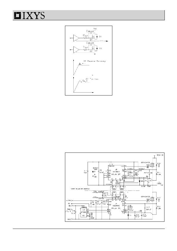
�stances.� When� switching� a� clamped�
�inductive� load� (Fig.� 5),� the� turn-on� of�
�Q2� will� commutate� the� freewheeling�
�diode� around� Q1.� Whether� this� diode� is�
�intrinsic� (as� in� a� MOSFET)� or� extrinsic�
�(IGBT� or� bipolar),� its� reverse� recovery�
�is� critical� to� proper� circuit� operation.�
�At� high� turn-on� di/dt� in� Q2� and� near� its�
�rated� voltage,� the� recovery� of� D1� can�
�get� quite� "snappy"� (the� di/dt� in� the�
�second� half� of� the� recovery� process,�
�after� the� diode� has� begun� to� recover� its�
�blocking� capability,� can� get� very� large),�
�creating� a� very� high� dv/dt� across� Q1.�
�This� dv/dt� is� impressed� across� the�
�Miller� capacitance� of� Q1,� forcing� a�
�Fig.� 5:� Switching� a� clamped� inductive�
�load�
�terminal� of� the� device.� If� this� current�
�pulse� causes� a� high� enough� voltage�
�drop� across� the� output� impedance� of�
�the� gate� drive� circuit,� R� out� ,� Q1� will� be�
�turned� on.�
�The� Q1� conduction� in� every� instance�
�Q2� is� turned� on� (and� vice� versa),� aside�
�from� degrading� efficiency,� can� lead� to�
�catastrophic� failure� of� both� power�
�transistors.� At� high� temperature,� where�
�the� -6� to� -7� mV/� °� C� temperature�
�coefficient� of� IGBT/MOSFET� threshold�
�may� be� required� to� achieve� the�
�necessary� RBSOA.� At� the� same� time,� it�
�is� mandatory� to� keep� the� off-state� gate�
�drive� impedance� very� low� to� assure� the�
�transistor� remain� off� during� induced�
�dv/dt� (including� diode� recovery� dv/dt).�
�In� some� instances,� it� is� simply� not�
�possible� to� satisfy� both� criteria� with� 0� V�
�applied� in� the� off-state.� In� these� cases�
�the� IXBD4410/4411� with� V� EE� negative�
�bias� generator� must� be� used.�
�The� internal� V� EE� generator� is� a� charge�
�pump� circuit.� Referring� to� Fig.� 6,� an�
�external� charge� pump� capacitor� is�
�required� between� the� CA� and� CB�
�1N5817�
�1N5817�
�large� current� to� flow� out� the� gate�
�?� 2004� IXYS� All� rights� reserved�
�Fig.� 6:� IXBD4410/4411� Detailed� one� phase� circuit� with� dead� time� generator� IXDP� 630�
�7�
�相关PDF资料 |
PDF描述 |
|---|---|
| LXC100-2800SW | POWER SUPPLY LED 100W 2800MA |
| R0.25D12-1515/H-R | CONV DC/DC 0.25W 15VIN +/-15VOUT |
| 346-062-526-201 | CARDEDGE 62POS DUAL .125 GREEN |
| AT88CK9000-8MA | CRYPTO PROGRAMMER BOARD 8-UDFN |
| VI-J3D-CW-F2 | CONVERTER MOD DC/DC 85V 100W |
相关代理商/技术参数 |
参数描述 |
|---|---|
| IXBD4411 | 制造商:IXYS 制造商全称:IXYS Corporation 功能描述:ISOSMART Half Bridge Driver Chipset |
| IXBD4411PC | 制造商:未知厂家 制造商全称:未知厂家 功能描述:Interface IC |
| IXBD4411PI | 功能描述:功率驱动器IC 1/2Bridge2A RoHS:否 制造商:Micrel 产品:MOSFET Gate Drivers 类型:Low Cost High or Low Side MOSFET Driver 上升时间: 下降时间: 电源电压-最大:30 V 电源电压-最小:2.75 V 电源电流: 最大功率耗散: 最大工作温度:+ 85 C 安装风格:SMD/SMT 封装 / 箱体:SOIC-8 封装:Tube |
| IXBD4411SI | 功能描述:功率驱动器IC 1/2Bridge2A RoHS:否 制造商:Micrel 产品:MOSFET Gate Drivers 类型:Low Cost High or Low Side MOSFET Driver 上升时间: 下降时间: 电源电压-最大:30 V 电源电压-最小:2.75 V 电源电流: 最大功率耗散: 最大工作温度:+ 85 C 安装风格:SMD/SMT 封装 / 箱体:SOIC-8 封装:Tube |
| IXBD4412PC | 制造商:未知厂家 制造商全称:未知厂家 功能描述:Interface IC |
发布紧急采购,3分钟左右您将得到回复。