- 您现在的位置:买卖IC网 > PDF目录20502 > IXBD4411PI (IXYS)IC HIGH SIDE DRIVER 16DIP PDF资料下载
参数资料
| 型号: | IXBD4411PI |
| 厂商: | IXYS |
| 文件页数: | 10/11页 |
| 文件大小: | 0K |
| 描述: | IC HIGH SIDE DRIVER 16DIP |
| 产品变化通告: | Discontinuation Notice 15/Jun/2010 |
| 标准包装: | 25 |
| 系列: | ISOSMART™ |
| 配置: | 高端 |
| 输入类型: | 非反相 |
| 延迟时间: | 110ns |
| 电流 - 峰: | 2A |
| 配置数: | 1 |
| 输出数: | 1 |
| 高端电压 - 最大(自引导启动): | 1200V |
| 电源电压: | 10 V ~ 20 V |
| 工作温度: | -40°C ~ 85°C |
| 安装类型: | 通孔 |
| 封装/外壳: | 16-DIP(0.300",7.62mm) |
| 供应商设备封装: | 16-DIP |
| 包装: | 管件 |
�� �
�
�IXBD4410�
�IXBD4411�
�If� the� MOSFET� switched� 25� A,� the�
�transient� will� last� as� long� as� (25/500)� μ� s�
�or� 50� ns,� which� is� more� than� the� typical�
�6� or� 7� ns� propagations� or� of� a� 74HC�
�series� gate.�
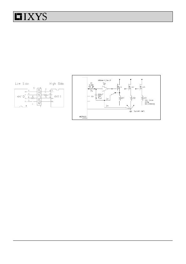
�Fig.� 10� illustrates� an� example� layout�
�problem.� The� power� circuit� consists� of�
�three� power� transistors� (MOSFETs� in�
�this� example).� With� the� ISOSMART?�
�gate� driver� chipset� grounded� as� in�
�option� (b)� in� Fig.� 10,� the� communication�
�path� from� the� IXDP630� will� operate�
�without� errors.� The� PC� trace� induced�
�voltages� are� not� common� with� the� digital�
�Fig.� 9:� Suggested� IC� Orientation�
�path,� so� the� input� of� the� gate� driver� will�
�drive� output� follows� (after� its� propaga-�
�tion� delay)� and� the� MOSFET� starts� to�
�conduct.� The� voltage� transient� induced�
�across� LS1� (V� =� LS1� ?� di/dt)� raises� the�
�local� ground� (point� a)� until� it� exceeds�
�V� oh� (630)� -� V� il� and� the� driver� (after� its�
�propagation� delay)� turns� the� MOSFET�
�off.� Now� the� MOSFET� current� falls,�
�V(LS1)� drops,� point� (a)� drops� to� system�
�ground� (or� slightly� below),� and� the� driver�
�detects� a� "1"� at� its� input.� After� its�
�propagation� delay,� it� again� turns� the�
�conversion� equipment� due� to� their� very�
�high� common� mode� dv/dt� rejection�
�capabilities.�
�Transformer� Considerations�
�The� transformer� is� the� communication�
�link� and� isolation� barrier� between� the�
�high-� and� low-side� ICs.� The� high-side�
�gate� and� fault� signals� are� transmitted�
�through� the� transformer� while� main-�
�taining� the� proper� isolation.� The�
�transmitter� signal� is� in� the� form� of� a�
�not� see� or� respond� to� them.�
�Fig.� 10:� Potential� layout� problems� that� create� functional� problems�
�Unfortunately,� the� MOSFET� will� not�
�operate� properly.� The� voltage� induced�
�across� LS1� when� Q1� is� turned� on,� acts�
�as� source� degeneration,� modifying� the�
�turn-on� behavior� of� the� MOSFET.� If�
�LS1=� 27� nH,� and� V� CC� is� 15� V� (assuming�
�the� gate� plateau� of� the� MOSFET� is� 6� V),�
�the� di/dt� at� turn-on� will� be� regulated� by�
�the� driver/MOSFET/LS1� loop� to� about�
�200� A/� μ� s;� quite� a� surprise� when� your�
�circuit� requires� 500� A/� μ� s� to� operate�
�correctly.�
�It� is� possible� to� make� use� of� this�
�behavior� to� create� a� turn-on� or� turn-off�
�di/dt� limiter� (perhaps� to� snub� the� upper�
�free� wheeling� diode� reverse� recovery).�
�While� possible,� this� is� normally� not�
�desirable� or� practical� where� two� or� more�
�transistors� are� controlled.� Equalizing� the�
�parasitic� impedances� of� three� traces�
�while� positioning� the� transistors� next� to�
�their� heat� sink� and� meeting� UL/VDE�
�voltage� spacings� is� just� too� difficult.�
�Grounding� the� gate� driver� as� in� option�
�(a)� in� Fig.� 10� solves� the� MOSFET� turn�
�on� problem� by� eliminating� LS1� from� the�
�source� feedback� loop.� Now,� unfor-�
�tunately,� the� gate� driver� will� oscillate�
�every� time� it� is� turned� on� or� off.� As� the�
�IXDP630� output� goes� "high",� the� gate�
�MOSFET� on,� continuing� the� oscillation�
�for� one� more� cycle.�
�To� eliminate� this� problem,� a� ground�
�level� transformation� circuit� must� be�
�added,� that� rejects� this� common� mode�
�transient.� The� simplest� is� a� de-coupling�
�circuit,� also� illustrated� in� Fig.� 10.� The�
�capacitor� voltage� on� C� d� remains�
�constant� while� the� transient� voltage� is�
�dropped� across� R� d� and� the� driver�
�detects� no� input� transition,� eliminating�
�the� oscillation.� This� circuit� does� add�
�significantly� to� turn-on� and� turn-off� delay�
�time,� and� cannot� be� used� if� the� transient�
�lasts� longer� than� the� allowable� delays.�
�Delay� times� must� be� considered� in�
�selection� of� system� dead� time.�
�The� most� complex� (and� most� effective)�
�method� of� eliminating� the� effects� of�
�transients� between� grounds� is� isolation.�
�Optocouplers� and� pulse� transformers�
�are� the� most� commonly� used� isolation�
�techniques,� and� work� very� well� in� this�
�case.� The� IXDP630/631� has� been�
�specifically� designed� to� directly� drive� a�
�high� speed� optocoupler� like� the� Hewlett�
�Packard� HCPL22XX� family� or� the�
�General� Instrument� 740L60XX� optologic�
�family.� These� optos� are� especially� well�
�suited� to� motor� control� and� power�
�square� wave,� but� the� receiver� responds�
�only� to� the� logic� edges.� This� allows� for�
�much� smaller� transformer� designs,�
�since� a� 10� kHz� switching� frequency�
�does� not� require� a� 10� kHz� pulse�
�transformer.�
�The� recommended� transformer� for� this�
�ISOSMART?� driver� chipset� is�
�fabricated� using� a� very� small� ferrite�
�shield� bead� (see� Fig.� 11),� onto� which� a�
�six-turn� primary� and� a� two-turn�
�secondary� winding� of� 36� AWG� magnet�
�wire� are� made.� The� two� windings� are�
�segment� wound� to� achieve� primary-to-�
�secondary� isolation� of� up� to� 2500� V~.�
�The� six-turn� primaries� are� connected� to�
�the� respective� IXBD4410/4411�
�transmitter� outputs� and� the� two-turn�
�secondaries� are� connected� to� their�
�respective� receiver� inputs.�
�?� 2004� IXYS� All� rights� reserved�
�相关PDF资料 |
PDF描述 |
|---|---|
| LXC120-1750SW | POWER SUPPLY LED 120W 1750MA |
| 346-062-540-802 | CARDEDGE 62POS DUAL .125 GREEN |
| 346-062-540-204 | CARDEDGE 62POS DUAL .125 GREEN |
| R0.25D12-1515/P-R | CONV DC/DC 0.25W 15VIN +/-15VOUT |
| 346-062-540-201 | CARDEDGE 62POS DUAL .125 GREEN |
相关代理商/技术参数 |
参数描述 |
|---|---|
| IXBD4411SI | 功能描述:功率驱动器IC 1/2Bridge2A RoHS:否 制造商:Micrel 产品:MOSFET Gate Drivers 类型:Low Cost High or Low Side MOSFET Driver 上升时间: 下降时间: 电源电压-最大:30 V 电源电压-最小:2.75 V 电源电流: 最大功率耗散: 最大工作温度:+ 85 C 安装风格:SMD/SMT 封装 / 箱体:SOIC-8 封装:Tube |
| IXBD4412PC | 制造商:未知厂家 制造商全称:未知厂家 功能描述:Interface IC |
| IXBD4412PI | 制造商:未知厂家 制造商全称:未知厂家 功能描述:Interface IC |
| IXBD4413PC | 制造商:未知厂家 制造商全称:未知厂家 功能描述:Interface IC |
| IXBD4413PI | 制造商:未知厂家 制造商全称:未知厂家 功能描述:Interface IC |
发布紧急采购,3分钟左右您将得到回复。