- 您现在的位置:买卖IC网 > PDF目录261629 > JCLGCATN3.686 (VECTRON INTERNATIONAL) VCXO, CLOCK, 3.686 MHz, CMOS/TTL OUTPUT PDF资料下载
参数资料
| 型号: | JCLGCATN3.686 |
| 厂商: | VECTRON INTERNATIONAL |
| 元件分类: | XO, clock |
| 英文描述: | VCXO, CLOCK, 3.686 MHz, CMOS/TTL OUTPUT |
| 封装: | ROHS COMPLIANT, HERMETIC SEALED, J-LEADE, CERAMIC, SOJ-6 |
| 文件页数: | 7/10页 |
| 文件大小: | 200K |
| 代理商: | JCLGCATN3.686 |
J-Type Voltage Controlled Crystal Oscillator
Vectron International 267 Lowell Rd. Hudson, NH 03051
Tel:1-88-VECTRON-1
e-mail vectron@vectron.com
6
Table 7. Standard Frequencies, in MHz, for CMOS output option
1.024
1.544
2.000
2.048
3.088
3.580
3.686
4.000
4.032
4.096
4.434
5.000
6.144
6.176
6.312
6.400
8.000
8.192
8.448
10.000
12.000
12.288
12.352
13.000
14.318
15.360
15.440
16.000
16.384
18.432
19.440
20.000
20.480
24.000
24.576
24.704
27.000
30.000
32.000
32.768
34.368
35.328
38.880
40.000
40.960
44.736
50.000
51.840
52.000
62.208
65.536
77.760
155.520
1
1. Uses a PLL multiplier, jitter is 25ps rms typical vs 3ps typical for a HFF design
Other frequencies available upon request.
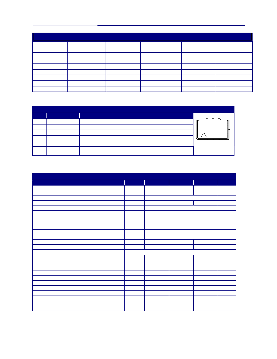
Table 8. Pin Out Information for the PECL output option
Pin
Symbol
Function
1
VC
VCXO Control Voltage
2
N/C or E/D
2
No Connect or Output Disable
3
GND
Case and Electrical Ground
4
Output
VCXO Output
5
COutput
VCXO Complementary Output
6
VCC
Power Supply Voltage (5.0 V or 3.3 V
±10%)
. By setting OD high, the outputs are disabled and OUT is held low while Complementary OUT is held high. Output is enabled if E/D
< VCC-1.6V,
2. See ordering information for enable/disable option.
Table 9. Electrical Performance @ 25
°C for the PECL output option
Parameter
Symbol
Minimum
Typical
Maximum
Units
Supply Voltage
1, +5 volt option
+3.3 volt option
4.5
3.0
5.0
3.3
5.5
3.6
V
Supply Current
frequency dependent
Center Frequency, see ordering information
FN
15
170
MHz
Operating Temperature, see ordering info
TOP
0/70, -40/85
°C
Absolute Pull Range over the operating
temperature range, aging and power supply.
Vc= 0.5 to 4.5 or 0.3 to 3.0
see ordering information for options
APR
±32, ±50
ppm
Gain Transfer
(Frequency vs. Control Voltage)
KV
Positive
Output Level High
2
VOH
Vcc-1.025
-
Vcc-0.880
V
Output Level Low
2
VOL
Vcc-1.810
-
Vcc-1.620
V
Output Logic Levels for -40 to 85
°C Operation
Output Level High
2
VOH
Vcc-1.085
Vcc-0.880
V
Output Level Low
2
VOL
Vcc-1.830
Vcc-1.555
V
Output Rise and Fall Time
2
tR/tf
1
ns
Duty Cycle
3, see ordering info
SYM
45/55
%
Input Leakage
IL
0.1
mA
RMS Jitter, 12kHz to 20 MHz, P option (HFF)
<1
pS
Control Voltage Modulation Bandwidth
BW
10
kHz
Maximum Control Voltage
0
VDD
Maximum Supply Voltage
7
V
Storage Temperature
TS
-55
-
125
°C
Soldering Temp./Time
TLS
-
240/10
°C/s
1. Power supply bypass is required and a 0.1uF in parallel with a 0.01uF high frequency capacitor is recommended.
2. Transition times are measured from 20% to 80% of a full 10K ECL level swing.
65
4
3
2
1
TOP VIEW
相关PDF资料 |
PDF描述 |
|---|---|
| JCLGCATN8.448 | VCXO, CLOCK, 8.448 MHz, CMOS/TTL OUTPUT |
| JCLCLD-34.368MHZ | VCXO, CLOCK, 34.368 MHz, CMOS OUTPUT |
| JDLHLA-37.056MHZ | VCXO, CLOCK, 37.056 MHz, TTL OUTPUT |
| JDLHLA-FREQ-OUT3 | VCXO, CLOCK, 0.000183 MHz - 155.52 MHz, TTL OUTPUT |
| JDLHLD-27.300MHZ | VCXO, CLOCK, 27.3 MHz, CMOS OUTPUT |
相关代理商/技术参数 |
参数描述 |
|---|---|
| JCL-J1N | 制造商:Leach International Corporation 功能描述:MID RANGE - Bulk |
| JCL-J2A | 制造商:Leach International Corporation 功能描述:MID RANGE - Bulk |
| JCL-J7N | 制造商:Leach International Corporation 功能描述:MID RANGE - Bulk |
| JCLX36JTOP20ID M8.4 | 功能描述:处理器 - 专门应用 IDENT RoHS:否 制造商:Freescale Semiconductor 类型:Multimedia Applications 核心:ARM Cortex A9 处理器系列:i.MX6 数据总线宽度:32 bit 最大时钟频率:1 GHz 指令/数据缓存: 数据 RAM 大小:128 KB 数据 ROM 大小: 工作电源电压: 最大工作温度:+ 95 C 安装风格:SMD/SMT 封装 / 箱体:MAPBGA-432 |
| JCLX80JTOP11ID MCC8 | 功能描述:处理器 - 专门应用 IDENT RoHS:否 制造商:Freescale Semiconductor 类型:Multimedia Applications 核心:ARM Cortex A9 处理器系列:i.MX6 数据总线宽度:32 bit 最大时钟频率:1 GHz 指令/数据缓存: 数据 RAM 大小:128 KB 数据 ROM 大小: 工作电源电压: 最大工作温度:+ 95 C 安装风格:SMD/SMT 封装 / 箱体:MAPBGA-432 |
发布紧急采购,3分钟左右您将得到回复。