- 您现在的位置:买卖IC网 > PDF目录261641 > JCLHCATNAT77.76MHZ (VECTRON INTERNATIONAL) VCXO, CLOCK, 77.76 MHz, PECL OUTPUT PDF资料下载
参数资料
| 型号: | JCLHCATNAT77.76MHZ |
| 厂商: | VECTRON INTERNATIONAL |
| 元件分类: | XO, clock |
| 英文描述: | VCXO, CLOCK, 77.76 MHz, PECL OUTPUT |
| 文件页数: | 2/8页 |
| 文件大小: | 121K |
| 代理商: | JCLHCATNAT77.76MHZ |
J-Type Voltage Controlled Crystal Oscillator
Vectron International 267 Lowell Road, Hudson, NH 03051 Tel: 1-88-VECTRON-1 Fax: 1-888-FAX-VECTRON
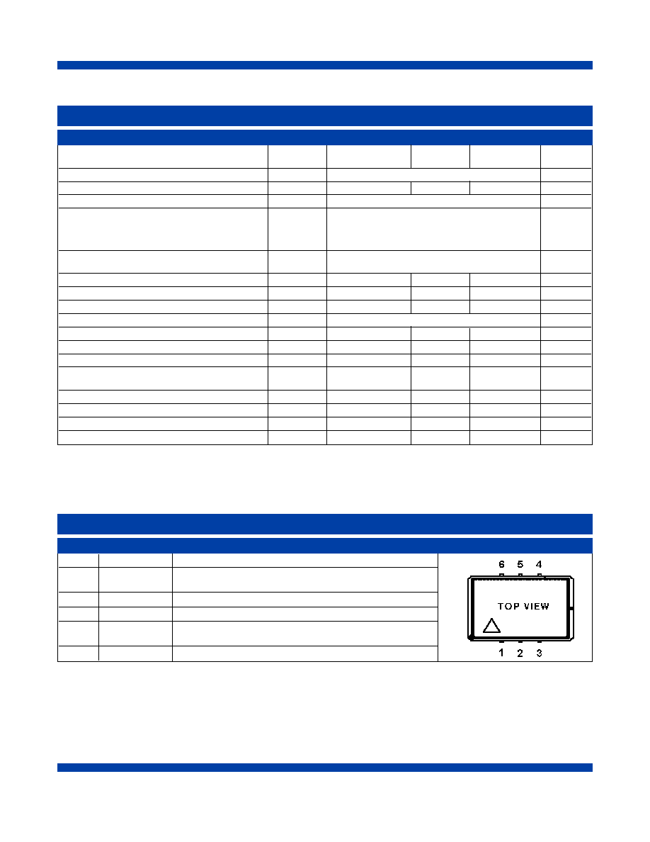
1
Vc
VCXO Control Voltage.
2
Tri-State1
TTL logic low disables output
TTL logic high, or no connect, enables output
3
GND
Case and electrical ground.
4
Output
VCXO Output
5
CMOS/TTL
TTL logic low optimizes symmetry for CMOS
select1,2
TTL logic high, or NC, optimizes symmetry for TTL.
6VCC
Power Supply Voltage (5.0 V or 3.3V ±10%)
Pin Out Information for the CMOS output option
Electrical Performance @ 25°C for the CMOS output option
CMOS Output Option
1. Standard option. Tri-State can be connected to pin 5 and CMOS/TTL select would be on pin 2.
2. Output is HCMOS. For frequencies >12MHz, this option optimizes symmetry for either CMOS or TTL thresholds. Ground this pin for fre-
quencies < 12MHz.
Supply Voltage1, +5 volt option
4.5
5.0
5.5
Vdc
+3.3 volt option
3.0
3.3
3.6
Vdc
Supply Current
10mA + 0.25mA per MHz, typical
Center Frequency, see ordering information
FN
1.024
77.760
MHz
Operating Temperature, see ordering info
TOP
0/70, -40/85
°C
Absolute Pull Range over the operating tempera-
APR
±50 to ±100
ppm
ture range, aging and power supply Vc=0.5 to
4.5 at 5V supply or 0.3 to 3.0 V at 3.3V supply
see ordering information for options
Gain Transfer
KV
Positive
(Frequency vs. Control Voltage)
Output Level High2
VOH
0.8*Vcc
-
V
Output Level Low2
VOL
-
0.1*Vcc
V
Output Rise/Fall Time2
tR/ tF
5ns
Duty Cycle3, see ordering info
SYM
45/55 or 40/60
%
Control Input Leakage
IL
1uA
Control Voltage Modulation Bandwidth
BW
-
10
-
kHz
RMS Jitter, Output=12.0-77.760 MHz
3ps
RMS Jitter, Output =12.0-77.760 MHz.
<0.5
ps
Band =12.0 KHz - 20 MHz
Control Range
0
VDD
Maximum Supply Voltage
7V
Storage Temperature
TS
-55
-
125
°C
Soldering Temp./Time
TLS
-
220/10
°C/s
2
Parameter
Symbol
Minimum
Typical
Maximum
Unit
1. Power supply bypass is required and a 0.1uF in parallel with a 0.01uF high frequency capacitor is recommended.
2. Figure 1 defines these parameters. Figure 2 illustrates the load used to test devices.
3. Duty cycle is defined as on-time versus period at 1.4 V for TTL, and 2.5 V for CMOS (5volt supply) and at 1.65 V for CMOS (3.3 volt operation)
Pin
Symbol
Function
相关PDF资料 |
PDF描述 |
|---|---|
| JCUGLMUNAT155.52MHZ | VCXO, CLOCK, 155.52 MHz, PECL OUTPUT |
| JCUGLMUTAT155.52MHZ | VCXO, CLOCK, 155.52 MHz, PECL OUTPUT |
| JDLGCKTNAT4.032MHZ | VCXO, CLOCK, 4.032 MHz, CMOS OUTPUT |
| JDLGCKTNAT52MHZ | VCXO, CLOCK, 52 MHz, CMOS OUTPUT |
| JCUGCJTNAT8.192MHZ | VCXO, CLOCK, 8.192 MHz, CMOS OUTPUT |
相关代理商/技术参数 |
参数描述 |
|---|---|
| JCL-J1N | 制造商:Leach International Corporation 功能描述:MID RANGE - Bulk |
| JCL-J2A | 制造商:Leach International Corporation 功能描述:MID RANGE - Bulk |
| JCL-J7N | 制造商:Leach International Corporation 功能描述:MID RANGE - Bulk |
| JCLX36JTOP20ID M8.4 | 功能描述:处理器 - 专门应用 IDENT RoHS:否 制造商:Freescale Semiconductor 类型:Multimedia Applications 核心:ARM Cortex A9 处理器系列:i.MX6 数据总线宽度:32 bit 最大时钟频率:1 GHz 指令/数据缓存: 数据 RAM 大小:128 KB 数据 ROM 大小: 工作电源电压: 最大工作温度:+ 95 C 安装风格:SMD/SMT 封装 / 箱体:MAPBGA-432 |
| JCLX80JTOP11ID MCC8 | 功能描述:处理器 - 专门应用 IDENT RoHS:否 制造商:Freescale Semiconductor 类型:Multimedia Applications 核心:ARM Cortex A9 处理器系列:i.MX6 数据总线宽度:32 bit 最大时钟频率:1 GHz 指令/数据缓存: 数据 RAM 大小:128 KB 数据 ROM 大小: 工作电源电压: 最大工作温度:+ 95 C 安装风格:SMD/SMT 封装 / 箱体:MAPBGA-432 |
发布紧急采购,3分钟左右您将得到回复。