- 您现在的位置:买卖IC网 > PDF目录261627 > JDLHCJTN-32.768MHZ (VECTRON INTERNATIONAL) VCXO, CLOCK, 32.768 MHz, CMOS OUTPUT PDF资料下载
参数资料
| 型号: | JDLHCJTN-32.768MHZ |
| 厂商: | VECTRON INTERNATIONAL |
| 元件分类: | XO, clock |
| 英文描述: | VCXO, CLOCK, 32.768 MHz, CMOS OUTPUT |
| 封装: | HERMETICALLY SEALED, CERAMIC, SO-6 |
| 文件页数: | 1/2页 |
| 文件大小: | 71K |
| 代理商: | JDLHCJTN-32.768MHZ |
12
Vectron International 267 Lowell Road, Hudson, NH 03051 Tel: 1-88-VECTRON-1 Web: www.vectron.com
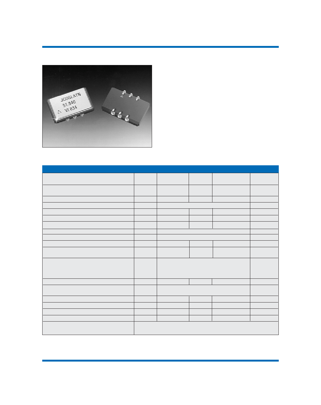
Voltage Controlled Crystal Oscillators (VCXO’s)
J-Type CMOS Output Option
Description:
The J-Type CMOS output option
is a high reliability CMOS VCXO, ASIC based and
available in a 6 or 4 pin J-Lead ceramic package.
Features:
Output Frequencies from 1.024 MHz to 77.76 MHz
3.3 or 5.0 volt options
Small 14mm x 9mm J-Lead Package
Low phase noise and custom options
0/70°C or –40/85°C operating temperature
Tri-state output (CMOS)
Center Frequency, see ordering information
fo
1.024
77.760
MHz
Supply Voltage1, +5.0 volt option
4.5
5.0
5.5
Vdc
+3.3 volt option
3.0
3.3
3.6
Vdc
Maximum Supply Voltage
7
V
Supply Current (frequency dependent)
10 mA +0.25 mA per MHz, typical
Output Level High
VOH
0.8*Vcc
-
V
Output Level Low
VOL
-
0.1*Vcc
V
Output Rise and Fall Time
tR/tF
5ns
Symmetry (Duty Cycle 2)
SYM
45/55 or 40/60
%
Operating Temperature, see ordering info
TOP
0/70, -40/85
°C
RMS Jitter, Output = 12.0-77.760 MHz
3
ps
RMS Jitter, Output = 12.0 -77.760 MHz,
Band = 12.0 kHz to 20 MHz
<0.5
ps
Absolute Pull Range over the operating
APR
±50, ±100
ppm
temperature range, aging and power supply.
Vc= 0.5 to 4.5 supply or 0.3 to 3.0V at 3.3V
supply. See ordering information for options
Control Range
0
VDD
Gain Transfer:
KV
Positive
(Frequency vs. Control Voltage)
Control Input Leakage
IL
1uA
Control Voltage Modulation Bandwidth
BW
10
kHz
Storage Temperature
TS
-55
-
125
°C
Soldering Temp./Time
TLS
-
220/10
°C/s
Package Size
14 x 9 x 4.5 mm
Parameter
Symbol
Minimum
Typical
Maximum
Unit
1. Power supply bypass is required and a 0.1uF in parallel with a 0.01uF high frequency capacitor is recommended.
2. Duty cycle is defined as on-time versus period at 1.4V for TTL and 2.5V for CMOS (5 volt supply) and at 1.65 V for CMOS
(3.3 volt operation)
Performance Characteristics
8798_AA's Vectron
05/30/02
3:11 PM
Page 12
相关PDF资料 |
PDF描述 |
|---|---|
| JDLHLATN-27MHZ | VCXO, CLOCK, 27 MHz, CMOS/TTL OUTPUT |
| JDUHLATN-77.76MHZ | VCXO, CLOCK, 77.76 MHz, CMOS/TTL OUTPUT |
| JDLGCATN4.434 | VCXO, CLOCK, 4.434 MHz, CMOS/TTL OUTPUT |
| JDLGCATN6.4 | VCXO, CLOCK, 6.4 MHz, CMOS/TTL OUTPUT |
| JDLGCJTN14.318 | VCXO, CLOCK, 14.318 MHz, CMOS OUTPUT |
相关代理商/技术参数 |
参数描述 |
|---|---|
| JDLI | 制造商:Thomas & Betts 功能描述:DIRECT BURIAL LAY IN GROUND CLAMP |
| JDLI-1 | 制造商:Thomas & Betts 功能描述:DIRECT BURIAL LAY IN GROUND CLAMP |
| JDLI-B1-10 | 制造商:Thomas & Betts 功能描述:3/8-1 GROUND CLAMP BRONZE LAYIN |
| JDLSLJTN-63.8976MHZ | 制造商:Vectron International 功能描述: |
| JDMGCMUX7776000MHZ | 制造商:Vectron International 功能描述: |
发布紧急采购,3分钟左右您将得到回复。