- 您现在的位置:买卖IC网 > PDF目录176123 > JDUHLA-32.768MHZ (VECTRON INTERNATIONAL) VCXO, CLOCK, 32.768 MHz, TTL OUTPUT PDF资料下载
参数资料
| 型号: | JDUHLA-32.768MHZ |
| 厂商: | VECTRON INTERNATIONAL |
| 元件分类: | VCXO, clock |
| 英文描述: | VCXO, CLOCK, 32.768 MHz, TTL OUTPUT |
| 文件页数: | 2/4页 |
| 文件大小: | 205K |
| 代理商: | JDUHLA-32.768MHZ |
J-Type Voltage Controlled Crystal Oscillator
www.vectron.com
USA: Vectron International 166 Glover Avenue, Norwalk, CT 06856 Tel: 1-88-VECTRON-1 Fax: 1-888-FAX-VECTRON
EUROPE: In Denmark, Finland, Ireland, Italy, Israel, Norway, Spain, UK: Tel: 44(0) 1703 766 288 Fax: 44 (0) 1703 766 822
In Austria, Belgium, France, Germany, Luxembourg, Netherlands, Sweden, Switzerland: Tel: 49 (0) 72 63 648 0 Fax: 49(0) 72 63 619 6
ASIA: In China, Taiwan, Japan: Tel: 1-603-598-0075 In Korea, Singapore, Australia, India: Tel: 1-203-853-4433 Fax: 1-203-849-1423
Vectron International reserves the right to make changes to the product(s) and/or information contained herein without notice.
No liability is assumed as a result of their use or application.
No rights under any patent accompany the sale of any such product(s) or information.
2
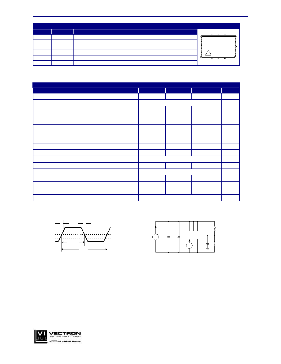
Pin Information
Table 1. Pin Function
Pin
Symbol
Function
1
VC
VCXO Control Voltage
2 (5)
1
N.C.
No User Connection
3
GND
Case Ground
4
Output
VCXO Output
5 (2)
1
Tri-State
TTL Low to Disable Output. TTL High or Float to Enable Output.
6
VDD
Power Supply Voltage (3.0 V
±10%, 3.3 V ±10% or 5.0 V ±10%)
1. Alternate pin configuration for tri-state control on pin2. Alternate configuration is indicated by the last letter of the code “D” as indicated in table 6.
Performance Characteristics
Table 2. Electrical Performance
Parameter
Symbol
Minimum
Typical
Maximum
Units
Supply Voltage
1
VDD
0.9* VDD
VDD
1.1* VDD
V
Supply Current
IDD
10 mA + 0.25 mA/MHz Typical
mA
Output Voltage Levels
2
Output High
Output Low
VOH
VOL
0.8*VDD
0.1* VDD
V
Transition times
2
Rise Time
Fall Time
TR
TF
5.0
ns
Duty Cycle
3
D
45
50
55
%
Nominal Output Frequency
4
f0
183E-6
155.52
MHz
Absolute Pull Range
APR
See Part Numbering and APR Section
ppm
Control Voltage
VC
0
VDD
V
Center Voltage
V0
Please Contact VTI for Details
V
Leakage Current of Control Input
IC
-1
1
A
Control Voltage Bandwidth (-3 dB, VC=0.5*VDD)
5
BW
10
kHz
Gain Slope @ V0
f/V
C
150
ppm/V
Phase Noise
φ
N
Contact VTI for Phase Noise Specifications
dBc/Hz
1. A 0.1
F low frequency tantalum bypass capacitor in parallel with a 0.01 F high frequency ceramic capacitor is recommended.
2. Figure 1 defines these parameters. Figure 2 illustrates the equivalent 5-gate TTL load and operating conditions under which these parameters are specified and tested.
3. Duty cycle is defined as (on time
÷period), with VS = 1.4 for TTL or VS = 2.5 V for CMOS, per Figure 1.
4. Other frequencies may be available, please contact factory with your special requirements.
5. Wider bandwidth versions are available, please contact VTI for details.
Figure 1. Output Waveform
Figure 2. Output Test Conditions (25
±±5°C)
Absolute Pull Range (APR) Specification
The frequency deviation of the J-Type VCXO is specified in
terms of Absolute Pull Range (APR). APR provides the user
with a guaranteed specification for minimum available
frequency deviation over all operating conditions. Operating
conditions include operating temperature range, power supply
variation, differences in output loading and changes due to
aging.
A J-Type VCXO with an APR of +/-50 ppm will track a +/-50
ppm reference source over all operating conditions. The
same device will typically demonstrate a Total Pull
capability of 150 to 350 ppm. Absolute Pull Range (APR) is
specified by the fourth character of the product code in Table
6. Please contact VTI for the APR Application Note.
Oscillator Aging
Quartz stabilized oscillators typically exhibit a small shift in
output frequency during aging. The major factors which lead to
this shift are changes in the mechanical stress on the crystal
and mass-loading of foreign material on the crystal.
0V
V
OH
V
S
V
OL
T
F
T
R
Period
On Time
+
-
+
-
I
C
V
C
4
3
.1
F
.01
F
15pF
2
5
6
1
I
DD
650
1.8k
V
DD
6
5
4
3
2
1
TOP VIEW
相关PDF资料 |
PDF描述 |
|---|---|
| JDUHLA-34.368MHZ | VCXO, CLOCK, 34.368 MHz, TTL OUTPUT |
| JDUHLJ-62.208MHZ | VCXO, CLOCK, 62.208 MHz, CMOS OUTPUT |
| JCUHCJ-49.152MHZ | VCXO, CLOCK, 49.152 MHz, CMOS OUTPUT |
| JCUHLA-32.768MHZ | VCXO, CLOCK, 32.768 MHz, TTL OUTPUT |
| JCUHLJ-77.760MHZ | VCXO, CLOCK, 77.76 MHz, CMOS OUTPUT |
相关代理商/技术参数 |
参数描述 |
|---|---|
| JDV2S01E | 制造商:TOSHIBA 制造商全称:Toshiba Semiconductor 功能描述:VCO for UHF band |
| JDV2S01E(TH3,F,T) | 制造商:Toshiba America Electronic Components 功能描述:Diode VAR Cap Single 10V 2.85pF 2-Pin ESC T/R |
| JDV2S01E-07 | 制造商:TOSHIBA 制造商全称:Toshiba Semiconductor 功能描述:Silicon Epitaxial Planar Type VCO for UHF band |
| JDV2S01ETH3FT | 功能描述:变容二极管 VARICAP DIODE RoHS:否 制造商:Skyworks Solutions, Inc. 电容:5.2 pF 反向电压:10 V 正向连续电流:20 mA 端接类型:SMD/SMT 封装 / 箱体:SC-79 封装:Reel |
| JDV2S01ETH3T | 制造商:Toshiba America Electronic Components 功能描述:VAR CAP SGL 10V 2.85PF 2PIN ESC - Bulk |
发布紧急采购,3分钟左右您将得到回复。