- 您现在的位置:买卖IC网 > PDF目录299245 > K4S281632D-TI7C 8M X 16 SYNCHRONOUS DRAM, 5.4 ns, PDSO54 PDF资料下载
参数资料
| 型号: | K4S281632D-TI7C |
| 元件分类: | DRAM |
| 英文描述: | 8M X 16 SYNCHRONOUS DRAM, 5.4 ns, PDSO54 |
| 封装: | 0.400 X 0.875 INCH, 0.80 MM PITCH, TSOP2-54 |
| 文件页数: | 9/9页 |
| 文件大小: | 80K |
| 代理商: | K4S281632D-TI7C |
CMOS SDRAM
K4S281632D
Rev. 0.1 Sept. 2001
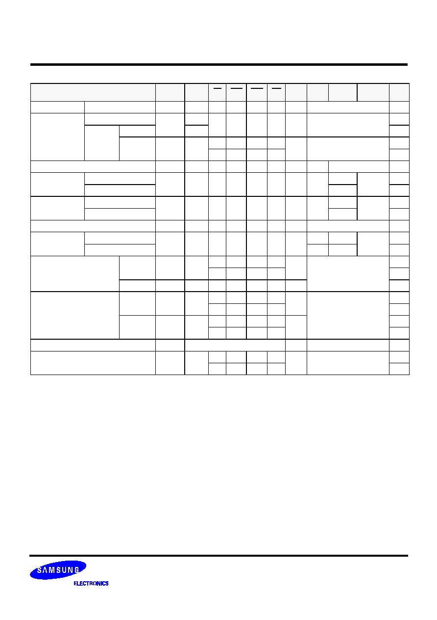
SIMPLIFIED TRUTH TABLE
Command
CKEn-1
CKEn
CS
RAS
CAS
WE
DQM
BA0,1
A10/AP
A11,
A9 ~ A0
Note
Register
Mode register set
H
X
L
X
OP code
1,2
Refresh
Auto refresh
H
L
H
X
3
Self
fefresh
Entry
L
3
Exit
L
H
L
H
X
3
H
X
3
Bank active & row addr.
H
X
L
H
X
V
Row address
Read &
column address
Auto precharge disable
H
X
L
H
L
H
X
V
L
Column
address
(A0 ~ A8)
4
Auto precharge enable
H
4,5
Write &
column address
Auto precharge disable
H
X
L
H
L
X
V
L
Column
address
(A0 ~ A8)
4
Auto precharge enable
H
4,5
Burst stop
H
X
L
H
L
X
6
Precharge
Bank selection
H
X
L
H
L
X
V
L
X
All banks
X
H
Clock suspend or
active power down
Entry
H
L
H
X
L
V
Exit
L
H
X
Precharge power down mode
Entry
H
L
H
X
L
H
Exit
L
H
X
L
V
DQM
H
X
V
X
7
No operation command
H
X
H
X
L
H
1. OP Code : Operand code
A0 ~ A11 & BA0 ~ BA1 : Program keys. (@ MRS)
2. MRS can be issued only at all banks precharge state.
A new command can be issued after 2 CLK cycles of MRS.
3. Auto refresh functions are as same as CBR refresh of DRAM.
The automatical precharge without row precharge command is meant by "Auto".
Auto/self refresh can be issued only at all banks precharge state.
4. BA0 ~ BA1 : Bank select addresses.
If both BA0 and BA1 are "Low" at read, write, row active and precharge, bank A is selected.
If both BA0 is "Low" and BA1 is "High" at read, write, row active and precharge, bank B is selected.
If both BA0 is "High" and BA1 is "Low" at read, write, row active and precharge, bank C is selected.
If both BA0 and BA1 are "High" at read, write, row active and precharge, bank D is selected.
If A10/AP is "High" at row precharge, BA0 and BA1 is ignored and all banks are selected.
5. During burst read or write with auto precharge, new read/write command can not be issued.
Another bank read/write command can be issued after the end of burst.
New row active of the associated bank can be issued at tRP after the end of burst.
6. Burst stop command is valid at every burst length.
7. DQM sampled at positive going edge of a CLK and masks the data-in at the very CLK (Write DQM latency is 0),
but makes Hi-Z state the data-out of 2 CLK cycles after. (Read DQM latency is 2)
Notes :
相关PDF资料 |
PDF描述 |
|---|---|
| K4S281632D-TP7C | 8M X 16 SYNCHRONOUS DRAM, 5.4 ns, PDSO54 |
| K50-3C0E35.3280MR | CRYSTAL OSCILLATOR, CLOCK, 35.328 MHz, CMOS OUTPUT |
| K50-3C1E27.0000MR | CRYSTAL OSCILLATOR, CLOCK, 27 MHz, CMOS OUTPUT |
| K50-3C1E53.125MR | CRYSTAL OSCILLATOR, CLOCK, 53.125 MHz, CMOS OUTPUT |
| K50-3C0E32MR | CRYSTAL OSCILLATOR, CLOCK, 32 MHz, CMOS OUTPUT |
相关代理商/技术参数 |
参数描述 |
|---|---|
| K4S281632D-TL75 | 制造商:SAMSUNG 制造商全称:Samsung semiconductor 功能描述:128Mbit SDRAM 2M x 16Bit x 4 Banks Synchronous DRAM LVTTL |
| K4S281632E-TC60 | 制造商:SAMSUNG 制造商全称:Samsung semiconductor 功能描述:128Mb E-die SDRAM Specification |
| K4S281632ETC75 | 制造商:Samsung Semiconductor 功能描述: |
| K4S281632E-TC75 | 制造商:SAMSUNG 制造商全称:Samsung semiconductor 功能描述:128Mb E-die SDRAM Specification |
| K4S281632ETC75000 FAB | 制造商:Custownprod 功能描述: |
发布紧急采购,3分钟左右您将得到回复。