参数资料
| 型号: | KAD2708L-27Q68 |
| 厂商: | Intersil |
| 文件页数: | 4/16页 |
| 文件大小: | 0K |
| 描述: | IC ADC 8BIT 275MSPS PAR 68-QFN |
| 产品培训模块: | High-Speed Analog-to-Digital Converters |
| 标准包装: | 1 |
| 系列: | FemtoCharge™ |
| 位数: | 8 |
| 采样率(每秒): | 275M |
| 数据接口: | 并联 |
| 转换器数目: | 1 |
| 功率耗散(最大): | 310mW |
| 电压电源: | 单电源 |
| 工作温度: | -40°C ~ 85°C |
| 安装类型: | 表面贴装 |
| 封装/外壳: | 68-VFQFN 裸露焊盘 |
| 供应商设备封装: | 68-QFN(10x10) |
| 包装: | 托盘 |
| 输入数目和类型: | 1 个差分,单极 |
12
FN6813.1
April 14, 2011
Functional Description
The KAD2708L is an 8-bit, 350MSPS A/D converter in a
pipelined architecture. The input voltage is captured by a
sample-and-hold circuit and converted to a unit of charge.
Proprietary charge-domain techniques are used to compare
the input to a series of reference charges. These
comparisons determine the digital code for each input value.
The converter pipeline requires 24 sample clocks to produce
a result. Digital error correction is also applied, resulting in a
total latency of 28 clock cycles. This is evident to the user as
a latency between the start of a conversion and the data
being available on the digital outputs.
At start-up, a self-calibration is performed to minimize gain
and offset errors. The reset pin (RST) is initially held low
internally at power-up and remains in that state until
calibration is complete. The clock frequency should remain
fixed during this time.
Calibration accuracy is maintained for the sample rate at
which it is performed and therefore should be repeated if the
clock frequency is changed by more than 10%. Recalibration
can be initiated via the RST pin, or power cycling, at any
time.
Reset
Recalibration of the ADC can be initiated at any time by
driving the RST pin low for a minimum of one clock cycle. An
open-drain driver is recommended.
The calibration sequence is initiated on the rising edge of
RST, as shown in Figure 21. The over-range output (ORP) is
set high once RST is pulled low, and it remains in that state
until calibration is complete. The ORP output returns to
normal operation at that time, so it is important that the
analog input be within the converter’s full-scale range in
order to observe the transition. If the input is in an
over-range state, the ORP pin stays high, and it is not
possible to detect the end of the calibration cycle.
While RST is low, the output clock (CLKOUTP/CLKOUTN)
stops toggling and is set low. Normal operation of the output
clock resumes at the next input clock edge (CLKP/CLKN)
after RST is deasserted. At 350MSPS, the nominal
calibration time is ~190ms.
Voltage Reference
The VREF pin is the full-scale reference, which sets the
full-scale input voltage for the chip and requires a bypass
capacitor of 0.1F or larger. An internally generated
reference voltage is provided from a bandgap voltage buffer.
This buffer can sink or source up to 50A externally.
An external voltage can be applied to this pin to provide a
more accurate reference than the internally generated
bandgap voltage or to match the full-scale reference among
a system of KAD2708L chips. One option in the latter
configuration is to use one KAD2708L's internally generated
reference as the external reference voltage for the other
chips in the system. Additionally, an externally provided
reference can be changed from the nominal value to adjust
the full-scale input voltage within a limited range.
To select whether the full-scale reference is internally
generated or externally provided, the digital input port,
VREFSEL, should be set appropriately: low for internal, or
high for external. This pin also has an internal 18k
Ω pull-up
resistor. To use the internally generated reference,
VREFSEL can be tied directly to AVSS, and to use an
external reference, VREFSEL can be left unconnected.
Analog Input
The fully differential ADC input (INP/INN) connects to the
sample-and-hold circuit. The ideal full-scale input voltage is
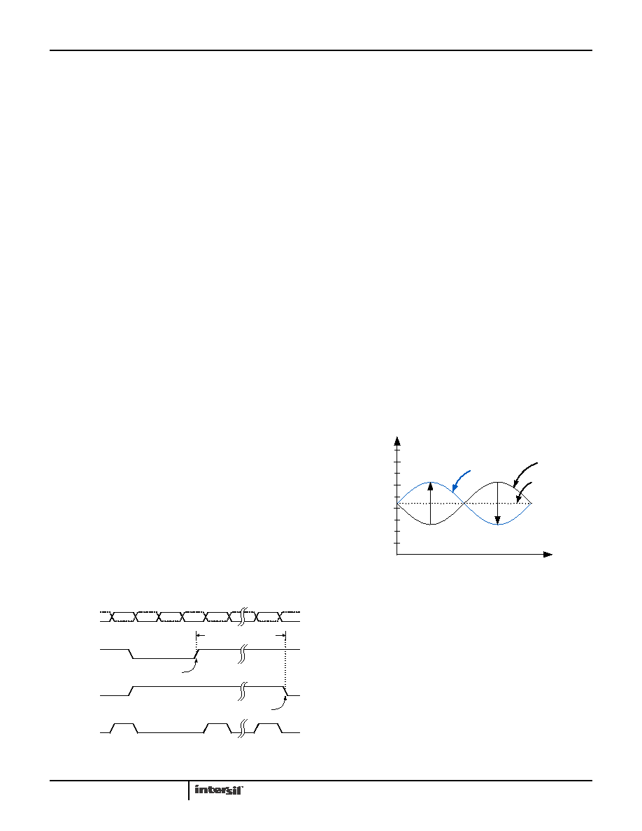
1.5VP-P, centered at the VCM voltage of 0.86V, as shown in
Figure 22.
Best performance is obtained when the analog inputs are
driven differentially. The common-mode output voltage,
VCM, should be used to properly bias each input, as shown
noise and distortion performance for wideband and/or high
intermediate frequency (IF) inputs. Two different transformer
FIGURE 21. CALIBRATION TIMING
CLKP
CLKN
CLKOUTP
RST
ORP
Calibration Begins
Calibration Complete
Calibration Time
FIGURE 22. ANALOG INPUT RANGE
1.0
1.8
0.6
0.2
1.4
INP
INN
VCM
0.86V
0.75V
-0.75V
V
t
KAD2708L
相关PDF资料 |
PDF描述 |
|---|---|
| KAD2710C-27Q68 | IC ADC 10BIT 275MSPS PAR 68-QFN |
| KAD2710L-21Q68 | IC ADC 10BIT 210MSPS SGL 68-QFN |
| KAD5510P-25Q48 | IC ADC 10BIT CMOS 250MSPS 48QFN |
| KAD5510P-50Q72 | IC ADC 10BIT 500MSPS SGL 72-QFN |
| KAD5512HP-17Q72 | IC ADC 12BIT 170MSPS SGL 72-QFN |
相关代理商/技术参数 |
参数描述 |
|---|---|
| KAD2708L-35Q68 | 功能描述:IC ADC 8BIT 350MSPS SGL 68-QFN RoHS:是 类别:集成电路 (IC) >> 数据采集 - 模数转换器 系列:FemtoCharge™ 产品培训模块:Lead (SnPb) Finish for COTS Obsolescence Mitigation Program 标准包装:1 系列:- 位数:10 采样率(每秒):357k 数据接口:DSP,MICROWIRE?,QSPI?,串行,SPI? 转换器数目:1 功率耗散(最大):830µW 电压电源:单电源 工作温度:-40°C ~ 85°C 安装类型:表面贴装 封装/外壳:10-WFDFN 裸露焊盘 供应商设备封装:10-TDFN-EP(3x3) 包装:剪切带 (CT) 输入数目和类型:2 个单端,单极;2 个单端,双极;1 个差分,单极;1 个差分,双极 产品目录页面:1396 (CN2011-ZH PDF) 其它名称:MAX1395ETB+TCT |
| KAD2710C | 制造商:INTERSIL 制造商全称:Intersil Corporation 功能描述:10-Bit, 275/210/170/105MSPS A/D Converter |
| KAD2710C-10Q68 | 功能描述:IC ADC 10BIT 105MSPS 68-QFN RoHS:是 类别:集成电路 (IC) >> 数据采集 - 模数转换器 系列:FemtoCharge™ 产品培训模块:Lead (SnPb) Finish for COTS Obsolescence Mitigation Program 标准包装:250 系列:- 位数:12 采样率(每秒):1.8M 数据接口:并联 转换器数目:1 功率耗散(最大):1.82W 电压电源:模拟和数字 工作温度:-40°C ~ 85°C 安装类型:表面贴装 封装/外壳:48-LQFP 供应商设备封装:48-LQFP(7x7) 包装:管件 输入数目和类型:2 个单端,单极 |
| KAD2710C-17Q68 | 功能描述:IC ADC 10BIT 170MSPS SGL 68-QFN RoHS:是 类别:集成电路 (IC) >> 数据采集 - 模数转换器 系列:FemtoCharge™ 产品培训模块:Lead (SnPb) Finish for COTS Obsolescence Mitigation Program 标准包装:250 系列:- 位数:12 采样率(每秒):1.8M 数据接口:并联 转换器数目:1 功率耗散(最大):1.82W 电压电源:模拟和数字 工作温度:-40°C ~ 85°C 安装类型:表面贴装 封装/外壳:48-LQFP 供应商设备封装:48-LQFP(7x7) 包装:管件 输入数目和类型:2 个单端,单极 |
| KAD2710C-21Q68 | 功能描述:IC ADC 10BIT 210MSPS SGL 68-QFN RoHS:是 类别:集成电路 (IC) >> 数据采集 - 模数转换器 系列:FemtoCharge™ 产品培训模块:Lead (SnPb) Finish for COTS Obsolescence Mitigation Program 标准包装:250 系列:- 位数:12 采样率(每秒):1.8M 数据接口:并联 转换器数目:1 功率耗散(最大):1.82W 电压电源:模拟和数字 工作温度:-40°C ~ 85°C 安装类型:表面贴装 封装/外壳:48-LQFP 供应商设备封装:48-LQFP(7x7) 包装:管件 输入数目和类型:2 个单端,单极 |
发布紧急采购,3分钟左右您将得到回复。