- 您现在的位置:买卖IC网 > PDF目录3944 > KMPC8313VRAGDB (Freescale Semiconductor)IC MPU POWERQUICC II 516-PBGA PDF资料下载
参数资料
| 型号: | KMPC8313VRAGDB |
| 厂商: | Freescale Semiconductor |
| 文件页数: | 20/99页 |
| 文件大小: | 0K |
| 描述: | IC MPU POWERQUICC II 516-PBGA |
| 标准包装: | 2 |
| 系列: | MPC83xx |
| 处理器类型: | 32-位 MPC83xx PowerQUICC II Pro |
| 速度: | 400MHz |
| 电压: | 0.95 V ~ 1.05 V |
| 安装类型: | 表面贴装 |
| 封装/外壳: | 516-BBGA 裸露焊盘 |
| 供应商设备封装: | 516-PBGAPGE(27x27) |
| 包装: | 托盘 |
第1页第2页第3页第4页第5页第6页第7页第8页第9页第10页第11页第12页第13页第14页第15页第16页第17页第18页第19页当前第20页第21页第22页第23页第24页第25页第26页第27页第28页第29页第30页第31页第32页第33页第34页第35页第36页第37页第38页第39页第40页第41页第42页第43页第44页第45页第46页第47页第48页第49页第50页第51页第52页第53页第54页第55页第56页第57页第58页第59页第60页第61页第62页第63页第64页第65页第66页第67页第68页第69页第70页第71页第72页第73页第74页第75页第76页第77页第78页第79页第80页第81页第82页第83页第84页第85页第86页第87页第88页第89页第90页第91页第92页第93页第94页第95页第96页第97页第98页第99页
MPC8313E PowerQUICC II Pro Processor Hardware Specifications, Rev. 4
Freescale Semiconductor
27
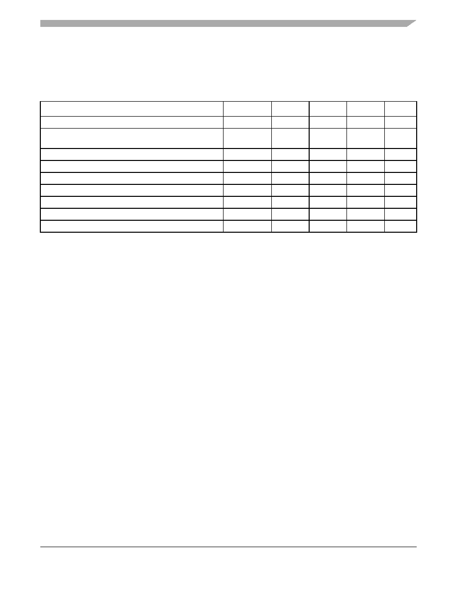
8.2.2
RGMII and RTBI AC Timing Specifications
This table presents the RGMII and RTBI AC timing specifications.
Table 30. RGMII and RTBI AC Timing Specifications
At recommended operating conditions with LVDDA/LVDDB of 2.5 V ± 5%.
Parameter/Condition
Symbol1
Min
Typ
Max
Unit
Data to clock output skew (at transmitter)
tSKRGT
–0.5
—
0.5
ns
Data to clock input skew (at receiver) 2
tSKRGT
1.0
—
2.6
ns
Clock cycle duration 3
tRGT
7.2
8.0
8.8
ns
Duty cycle for 1000Base-T 4, 5
tRGTH/tRGT
45
50
55
%
Duty cycle for 10BASE-T and 100BASE-TX 3, 5
tRGTH/tRGT
40
50
60
%
Rise time (20%–80%)
tRGTR
—
0.75
ns
Fall time (20%–80%)
tRGTF
—
0.75
ns
GTX_CLK125 reference clock period
tG12
6
—8.0
—
ns
GTX_CLK125 reference clock duty cycle
tG125H/tG125
47
—
53
%
Note:
1. Note that, in general, the clock reference symbol representation for this section is based on the symbols RGT to represent
RGMII and RTBI timing. For example, the subscript of tRGT represents the RTBI (T) receive (RX) clock. Note also that the
notation for rise (R) and fall (F) times follows the clock symbol that is being represented. For symbols representing skews,
the subscript is skew (SK) followed by the clock that is being skewed (RGT).
2. This implies that PC board design requires clocks to be routed such that an additional trace delay of greater than 1.5 ns is
added to the associated clock signal.
3. For 10 and 100 Mbps, tRGT scales to 400 ns ± 40 ns and 40 ns ± 4 ns, respectively.
4. Duty cycle may be stretched/shrunk during speed changes or while transitioning to a received packet's clock domains as
long as the minimum duty cycle is not violated and stretching occurs for no more than three tRGT of the lowest speed
transitioned between.
5. Duty cycle reference is LVDDA/2 or LVDDB/2.
6. This symbol is used to represent the external GTX_CLK125 and does not follow the original symbol naming convention.
7. The frequency of RX_CLK should not exceed the GTX_CLK125 by more than 300 ppm
相关PDF资料 |
PDF描述 |
|---|---|
| IDT70V5378S200BG | IC SRAM 576KBIT 200MHZ 272BGA |
| KMPC8313VRAFFB | IC MPU POWERQUICC II 516-PBGA |
| IDT70T653MS12BCI8 | IC SRAM 18MBIT 12NS 256BGA |
| IDT70V5378S200BC | IC SRAM 576KBIT 200MHZ 256BGA |
| IDT70T653MS15BC | IC SRAM 18MBIT 15NS 256BGA |
相关代理商/技术参数 |
参数描述 |
|---|---|
| KMPC8313ZQADDB | 功能描述:微处理器 - MPU 8313 REV2.1 W/O ENCR RoHS:否 制造商:Atmel 处理器系列:SAMA5D31 核心:ARM Cortex A5 数据总线宽度:32 bit 最大时钟频率:536 MHz 程序存储器大小:32 KB 数据 RAM 大小:128 KB 接口类型:CAN, Ethernet, LIN, SPI,TWI, UART, USB 工作电源电压:1.8 V to 3.3 V 最大工作温度:+ 85 C 安装风格:SMD/SMT 封装 / 箱体:FBGA-324 |
| KMPC8313ZQAFFB | 功能描述:微处理器 - MPU 8313 REV2.1 W/O ENCR RoHS:否 制造商:Atmel 处理器系列:SAMA5D31 核心:ARM Cortex A5 数据总线宽度:32 bit 最大时钟频率:536 MHz 程序存储器大小:32 KB 数据 RAM 大小:128 KB 接口类型:CAN, Ethernet, LIN, SPI,TWI, UART, USB 工作电源电压:1.8 V to 3.3 V 最大工作温度:+ 85 C 安装风格:SMD/SMT 封装 / 箱体:FBGA-324 |
| KMPC8314CVRAGDA | 功能描述:微处理器 - MPU NON-ENCRYPT RoHS:否 制造商:Atmel 处理器系列:SAMA5D31 核心:ARM Cortex A5 数据总线宽度:32 bit 最大时钟频率:536 MHz 程序存储器大小:32 KB 数据 RAM 大小:128 KB 接口类型:CAN, Ethernet, LIN, SPI,TWI, UART, USB 工作电源电压:1.8 V to 3.3 V 最大工作温度:+ 85 C 安装风格:SMD/SMT 封装 / 箱体:FBGA-324 |
| KMPC8314ECVRAGDA | 功能描述:微处理器 - MPU ENCRYPT RoHS:否 制造商:Atmel 处理器系列:SAMA5D31 核心:ARM Cortex A5 数据总线宽度:32 bit 最大时钟频率:536 MHz 程序存储器大小:32 KB 数据 RAM 大小:128 KB 接口类型:CAN, Ethernet, LIN, SPI,TWI, UART, USB 工作电源电压:1.8 V to 3.3 V 最大工作温度:+ 85 C 安装风格:SMD/SMT 封装 / 箱体:FBGA-324 |
| KMPC8314EVRAGDA | 功能描述:微处理器 - MPU ENCRYPT RoHS:否 制造商:Atmel 处理器系列:SAMA5D31 核心:ARM Cortex A5 数据总线宽度:32 bit 最大时钟频率:536 MHz 程序存储器大小:32 KB 数据 RAM 大小:128 KB 接口类型:CAN, Ethernet, LIN, SPI,TWI, UART, USB 工作电源电压:1.8 V to 3.3 V 最大工作温度:+ 85 C 安装风格:SMD/SMT 封装 / 箱体:FBGA-324 |
发布紧急采购,3分钟左右您将得到回复。